Contenuto principale

QSPI Peripheral Configuration

R2026b

Map QSPI peripherals in the Infineon AURIX model to peripheral registers in the MCU

Since R2024a

Description

Add-On Required: This feature requires the Embedded Coder Support Package for Infineon AURIX TC3x Microcontrollers add-on.

View and edit the map of peripheral blocks in the Infineon® AURIX™ model to the hardware peripherals.

Using the Hardware Mapping tool, you can:

  • View and edit configuration parameters for QSPI peripheral block.

  • Configure the global parameters. To set the group peripheral, select peripheral in Browser > Peripherals > QSPIPeripheral . For more, see Map Tasks and Peripherals Using Hardware Mapping.

  • Check for any conflicts between the peripherals.
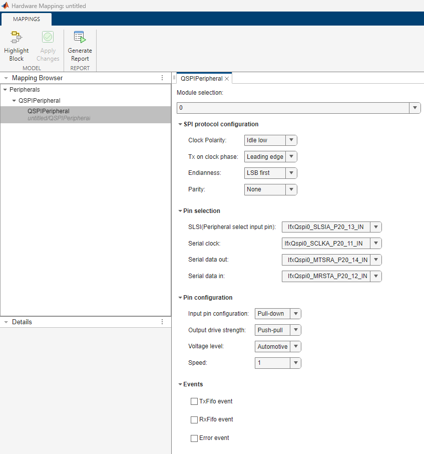
QSPI Peripheral mapping browser

Open the QSPI Peripheral Configuration

To open the Hardware Mapping tool, on the Simulink toolstrip, in the Hardware tab, click Hardware Mapping.

Hardware Mapping icon

Parameters

expand all

Module selection

Select the peripheral module for QSPI communication.

SPI protocol configuration

Specify the polarity of the clock signal received from the QSPI controller block.

Specify the clock edge of the clock signal received from the QSPI controller block.

Select the QSPI data heading in binary numbers.

  • LSB first — SDO pin outputs the least significant bit (LSB) first, then transmits the remaining bits from right to left.

  • MSB first — SDO pin transmits the most significant bit (MSB) first, then transmits the remaining bits from left to right.

Specify the clock parity of the clock signal received from the QSPI controller block.

Pin selection

Specify the pin number to receive the chip select signal from the QSPI controller block.

This parameter is read-only.

Specify the pin number to receive the serial clock signal from the QSPI controller block.

This parameter is read-only.

Specify the pin number to receive serial data from the QSPI Controller block.

This parameter is read-only.

Specify the pin number to transmit serial data to the QSPI Controller block.

Pin configuration

Specify input pin pull for the QSPI communication.

Specify drive strength for the QSPI output pin.

Specify voltage level for QSPI pin.

Select the pin speed for QSPI pins.

Events

Select to enable the QSPI transmit FIFO interrupt.

This parameter is read-only.

Select one of these operation modes for transmit FIFO buffer:

  • Single Move — Select this mode to generate an interrupt to refill the transmit buffer as soon as there is a free element.

  • Batch Move — Select this mode to generate an interrupt if the FIFO level of transmit data exceeds above TxFifo mode threshold value.

Dependencies

To enable this parameter, select the TxFifo event parameter.

Specify FIFO level for the Tx FIFO event.

Dependencies

To enable this parameter, select the TxFifo event parameter.

Enables the QSPI receive buffer interrupt.

This parameter is read-only.

Select one of these operation modes for the receive buffer:

  • Single Move — Select this mode to generate an interrupt to fetch the received element as soon as possible.

  • Batch Move — Select this mode to generate an interrupt if the filling level rises above RxFifo mode threshold value.

Dependencies

To enable this parameter, select the RxFifo event parameter.

Specify FIFO level for Rx FIFO event.

Dependencies

To enable this parameter, select the RxFifo event parameter.

Select to enables the QSPI error interrupt.

Version History

Introduced in R2024a