Cadnet-Level DC Power Integrity Analysis of PCIe 5.0 Allegro Board
This example demonstrates how to perform DC power integrity (PI-DC) analysis on a specific cadnet within a printed circuit board (PCB) design created using Cadence® Allegro. Using MATLAB, you can import the PCB layout, identify the power cadnet of interest, and analyze its DC performance. The goal is to ensure stable voltage delivery across the power distribution network (PDN), helping to prevent potential malfunctions or performance degradation in the board.
The first part of this example demonstrates how to import the PCB layout and select the cadnet of interest for PDN analysis. The second part walks through the setup and configuration of the PDN model, followed by performing DC power integrity analysis to evaluate voltage stability and current distribution across the selected cadnet.
Import the PCB Design
This example will use native files to import the PCB. if you want to enable the import of Allegro boards, set up path for extracta.exe using the below command:
LibraryPathPC = "Provide the path for Extracta.exe"
extractaSetup(LibraryPathPC)
Note: To keep this example focused and easy to work with, the surfaces.csv and traces_map.csv files in the Native folder have been tailored specifically for ‘P0V8’. These files include only the data relevant to this net: 'P0V8' , while still providing all essential information required for this example.
Once the board path is set, use the pcbFileRead object to import the Allegro board file into MATLAB. This object provides access to the PCB layout data, including components, nets, and layers. It enables you to extract a specific cadnet, which can then be used to construct a Power Distribution Network (PDN) model for performing DC power integrity (PI-DC) analysis.
BoardPath = "Provide the path for Allegro board"
pcb = pcbFileRead(BoardPath);
If you do not have Cadence® Allegro installed, follow the below steps to import the board using pcbFileRead with Native files as an input
% Use Native files to import the board
nativepath = fullfile(pwd,'Native');
pcb = pcbFileRead(nativepath)
pcb =
  pcbFileRead with properties:

           FileName: '/tmp/Bdoc26a_3233028_1144059/tp59e0d67a/rfpcb-ex28840861/Native'
          NumLayers: 41
         MetalLayer: [2 4 6 8 10 12 14 16 18 20 22 24 26 28 30 32 34 36 38 40]
    DielectricLayer: [1 3 5 7 9 11 13 15 17 19 21 23 25 27 29 31 33 35 37 39 41]
        LayerHeight: [0.0837 0.0817 0.0794 0.0782 0.0752 0.0746 0.0707 0.0695 0.0665 0.0659 0.0620 0.0608 0.0578 0.0572 0.0533 0.0521 0.0491 0.0485 0.0445 0.0433 0.0403 0.0391 0.0354 0.0348 0.0318 0.0306 0.0269 0.0263 0.0233 0.0221 … ] (1×41 double)
         NumCadnets: 3182
       NumPadStacks: 103
      NumComponents: 2852
           NumParts: 62
Once the board is imported, extract the list of Cadnets (Nets) available in the PCB using cadnetList. This function returns a complete list of nets present in the database, allowing you to browse power nets required for DC-PI analysis. To preview a small portion of the list, you can display only a specific row range. To view the full list, simply display NetList
NetList = cadnetList(pcb);
disp(NetList(1250:1260, :))
    CadnetIdx          CadnetName          NumPins    Length
    _________    ______________________    _______    ______

      1250       {'PGOOD_P1V8'        }        4      13.376
      1251       {'P0V8'              }      257       2.302
      1252       {'LCL_CLK01_100MHZ_P'}        4      18.981
      1253       {'LCL_CLK01_100MHZ_M'}        4      18.981
      1254       {'LCL_CLK00_100MHZ_P'}        4       13.47
      1255       {'LCL_CLK00_100MHZ_M'}        4      13.469
      1256       {'HOST_CLK_SEL1'     }        2       5.394
      1257       {'HOST_CLK_SEL0'     }        2       5.764
      1258       {'HOST_CLK_R_SEL0'   }        4       0.563
      1259       {'HOST_CLK_R_SEL1'   }        4       0.685
      1260       {'CXL_RX_DET_BYP_01' }        3       0.296
Select Power net from the list for PDN analysis
The PCIe 5.0 Allegro board uses the TPS546D24A voltage regulator module (VRM) to supply power to a load ASIC. The TPS546D24A is a highly integrated, non-isolated DC/DC converter capable of high frequency operation [1]. In this design, the SW (switching) pins of the TPS546D24A are connected to an output inductor, which acts as the primary energy delivery path. The output of this inductor feeds into the 'P0V8' net, a power rail that delivers 0.8 volts—a typical voltage level used in high-speed digital systems.
The 'P0V8' is one of the cadnet in the board that is responsible for powering critical components within the ASIC. Therefore, it forms a crucial part of the Power Distribution Network (PDN). By selecting and analyzing this cadnet, you can evaluate how much current is drawn by the ASIC pins and assess the DC power integrity of the rail. This helps ensure stable voltage delivery and prevents potential performance degradation or malfunction in the system.
Visualize the Power net 'P0V8'
use cadnet object to create the selected net and visualize it using show method
cadnetName = 'P0V8';
cnet = cadnet(pcb,cadnetName)
cnet =
cadnet with properties:
pcBoard: [1×1 pcbFileRead]
CadnetName: 'P0V8'
NumPins: 257
NumSurfaces: 16
NumVias: 399
NumTraces: 55
TotalLength: 2.3020
Voltage: '0.000'
LayerRange: [2 22 40]
EntityList: [1×1 struct]
show(cnet);
Adjust the axis ratio to expand Z-axis
ax = gca(cnet);
axis(ax,'equal');
daspect(ax,[1,1,0.05]);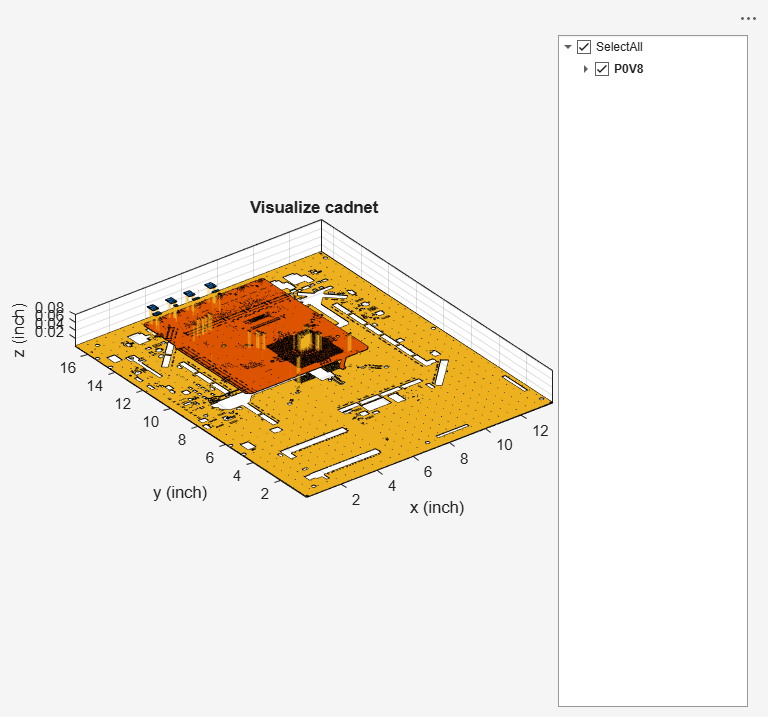
Use the findComponents method to analyze and retrieve details about all components that are electrically connected to a specific Cadnet in PCB design. This function is particularly useful when setting up Power Distribution Network (PDN) parameters, where understanding the component roles and pin connectivity is essential. The function supports optional filtering, enabling selective extraction of components, based on componentType which is useful when isolating specific categories, such as only capacitors for decoupling analysis and PartNumber helpful for narrowing the results to a particular device or manufacturer part.
Comp = findComponents(cnet)
Comp=123×5 table
    ComponentIndex    Refdes     PinList    ComponentType      Part
    ______________    _______    _______    _____________    _________

           1          "C1160"      "1"      {'Capacitor'}    {'CAPN' }
           2          "C1161"      "1"      {'Capacitor'}    {'CAPN' }
           3          "C1162"      "1"      {'Capacitor'}    {'CAPN' }
           4          "C1163"      "1"      {'Capacitor'}    {'CAPN' }
           5          "C1164"      "1"      {'Capacitor'}    {'CAPN' }
           6          "C1166"      "1"      {'Capacitor'}    {'CAPN' }
           7          "C1168"      "1"      {'Capacitor'}    {'CAPN' }
           8          "C1170"      "1"      {'Capacitor'}    {'CAPN' }
           9          "C1172"      "1"      {'Capacitor'}    {'CAPN' }
          10          "C1173"      "1"      {'Capacitor'}    {'CAPN' }
          11          "C1174"      "1"      {'Capacitor'}    {'CAPN' }
          12          "C1175"      "1"      {'Capacitor'}    {'CAP_P'}
          13          "C1176"      "1"      {'Capacitor'}    {'CAPN' }
          14          "C1177"      "1"      {'Capacitor'}    {'CAPN' }
          15          "C1178"      "1"      {'Capacitor'}    {'CAPN' }
          16          "C1179"      "1"      {'Capacitor'}    {'CAPN' }
      ⋮
Set up and Assignment for PDN
Create PDN model
To begin DC analysis, you need to create a PDN model for the cadnet of interest. MATLAB provides the powerDistributionNetwork object, which allows you to model and analyze the PDN based on the selected cadnet.
Use the following command to create the PDN object:
PDNModel = powerDistributionNetwork(cnet)
PDNModel =
  powerDistributionNetwork with properties:

   Network Parameters:
              NetType: [1×1 cadnet]
               Source: []
                 Load: []
                Sense: []
     PlatingThickness: []

   DC Parameters:
       NominalVoltage: []
          LoadCurrent: []

   DC Rules
    MaxCurrentDensity: []
           MinVoltage: []
           MaxVoltage: []
        MaxViaCurrent: []

To Analyse PDN:
Set Network Parameters: setNetworkParameters
Set DC Parameters: setDCParameters
Set DC Rules: setDCRules
Set up PDN Parameters
Once the PDN model is created, assign the relevant network components and electrical parameters. These include the source, load, sense point, and physical and electrical constraints.
Set Network parameters
To define the PDN topology for DC analysis, identify and assign the source, load, and sense pins using the findComponents function.
Source Pin
Use findComponents to locate all inductor connected to the cadnet. These typically represent the output stage of the VRM. Assign the pin of the L1 inductor as the source:
% Source Pin
SourceComp = findComponents(cnet,"ComponentType","Inductor")
SourceComp=4×5 table
    ComponentIndex    Refdes    PinList    ComponentType        Part
    ______________    ______    _______    _____________    ____________

          1            "L1"       "2"      {'Inductor'}     {'INDUCTOR'}
          2            "L2"       "2"      {'Inductor'}     {'INDUCTOR'}
          3            "L3"       "2"      {'Inductor'}     {'INDUCTOR'}
          4            "L4"       "2"      {'Inductor'}     {'INDUCTOR'}
sourcePin = SourceComp.Refdes(1)
sourcePin =
"L1"
Load Pin
Identify the ASIC (e.g., component U1) that draws current from the power net. The ASIC component U1 has 135 pins connected to the 'P0V8' cadnet, all of which act as load points in the PDN analysis.
% Load Pin
LoadComp = findComponents(cnet,"ComponentType","IC")
LoadComp=1×5 table
    ComponentIndex    Refdes                                                                                                                                                                                                                                                                                                                                                                                                                  PinList                                                                                                                                                                                                                                                                                                                                                                                                                   ComponentType          Part
    ______________    ______    ____________________________________________________________________________________________________________________________________________________________________________________________________________________________________________________________________________________________________________________________________________________________________________________________________________________________________________________________________________________________________________________________________________________________________________________________________________________________________________________________________________________________________________________________________________________________________________________________________________________________________    _____________    _________________

          1            "U1"     "AA20, AA22, AA24, AB19, AB21, AB23, AC20, AC22, AC24, AD19, AD21, AD23, AE20, AE22, AE24, AE41, AE43, AF19, AF21, AF23, AF42, AH25, AH27, AH29, AH31, AH33, AH35, AH37, AH39, AJ26, AJ28, AJ30, AJ32, AJ34, AJ36, AJ38, AJ40, AK25, AK27, AK29, AK31, AK33, AK35, AK37, AK39, AL26, AL28, AL30, AL32, AL34, AL36, AL38, AL40, AM25, AM27, AM29, AM31, AM33, AM35, AM37, AM39, AN26, AN28, AN30, AN32, AN34, AN36, AN38, AN40, AP25, AP27, AP29, AP31, AP33, AP35, AP37, AP39, AR26, AR28, AR30, AR32, AR34, AR36, AR38, AR40, AT25, AT27, AT29, AT31, AT33, AT35, AT37, AT39, AU26, AU28, AU30, AU32, AU34, AU36, AU38, AU40, AW19, AW21, AW23, AW42, AW44, AY20, AY22, AY24, AY41, AY43, BA19, BA21, BA23, BB20, BB22, BB24, BC19, BC21, BC23, BD20, BD22, BD24, BE19, BE21, BE23, BF20, BF22, BF24, W20, W22, W24, Y19, Y21, Y23"       {'IC'}        {'UV0261A-AS001'}
sinkPin = LoadComp.Refdes
sinkPin =
"U1"
Sense Pin
Select a resistor (e.g., R700) pin connected to the cadnet as the sense point, where the voltage is expected to match the nominal value (i.e., no voltage deviation):
% Sense Pin
senseComp = findComponents(cnet,"ComponentType","Resistor")
senseComp=2×5 table
    ComponentIndex    Refdes    PinList    ComponentType      Part
    ______________    ______    _______    _____________    ________

          1           "R106"      "2"      {'Resistor'}     {'RESN'}
          2           "R700"      "1"      {'Resistor'}     {'RESN'}
sensePin = senseComp.Refdes(2);
DC Inputs and constraints
% Load current
Idraw = 1;
% Max current density limit
Ilimit = 0.5;
% Nominal voltage
Vtarget = 0.8;
% plating thickness
platingThickness = 0.002;
Assign Parameters to the PDN Model
Use the following methods to assign the extracted values to the PDN model:
setNetworkParameters(PDNModel,Source=sourcePin,Load=sinkPin,Sense=sensePin,PlatingThickness=platingThickness);
  powerDistributionNetwork with properties:

   Network Parameters:
              NetType: [1×1 cadnet]
               Source: "L1"
                 Load: "U1"
                Sense: "R700"
     PlatingThickness: 0.0020

   DC Parameters:
       NominalVoltage: []
          LoadCurrent: []

   DC Rules
    MaxCurrentDensity: []
           MinVoltage: []
           MaxVoltage: []
        MaxViaCurrent: []

To Analyse PDN:
Set DC Parameters: setDCParameters
Set DC Rules: setDCRules
setDCParameters(PDNModel,"NominalVoltage",Vtarget,"LoadCurrent",Idraw);
  powerDistributionNetwork with properties:

   Network Parameters:
              NetType: [1×1 cadnet]
               Source: "L1"
                 Load: "U1"
                Sense: "R700"
     PlatingThickness: 0.0020

   DC Parameters:
       NominalVoltage: 0.8000
          LoadCurrent: 1

   DC Rules
    MaxCurrentDensity: []
           MinVoltage: []
           MaxVoltage: []
        MaxViaCurrent: []

To Analyse PDN:
Set DC Rules: setDCRules
setDCRules(PDNModel,"MaxCurrentDensity",Ilimit,"MaxVoltage",1,"MinVoltage",0.5,"MaxViaCurrent",1);
  powerDistributionNetwork with properties:

   Network Parameters:
              NetType: [1×1 cadnet]
               Source: "L1"
                 Load: "U1"
                Sense: "R700"
     PlatingThickness: 0.0020

   DC Parameters:
       NominalVoltage: 0.8000
          LoadCurrent: 1

   DC Rules
    MaxCurrentDensity: 0.5000
           MinVoltage: 0.5000
           MaxVoltage: 1
        MaxViaCurrent: 1
Run DC Simulation and Visualize Results
Voltage
To analyze voltage deviations across all points in your Power Distribution Network (PDN) relative to the nominal voltage (as specified earlier using setDCParameters), use the voltage method of the PDN object:
voltage(PDNModel);
Note:
This simulation may take longer to complete since the selected CAD net contains a large number of entities. For convenience, example screenshots of the simulated results are provided. However, you can run the voltage analysis yourself and interact with the resulting figure for deeper exploration.
Interactive Exploration
After running the voltage analysis and plotting the results, you can interactively explore the voltage behavior in the PDN.
click on
HighlightSourceandHighlightLoad.This will place data markers on the respective source and load locations on the PCB layout.
Turn on the Data Tip tool in the plot toolbar.
Click on the source and load markers to display detailed voltage information
It is observed that at the source pin, the voltage is measured at approximately 0.902 V, showing a deviation of 2.2 mV from the nominal voltage (0.9 V), and at the load pins (connected to the ASIC), the voltage is consistently around 0.89 V, indicating a voltage drop of approximately 7.3 mV from the source.
The voltage at all load pins remains uniform, suggesting a well-balanced PDN with minimal variation across the load.
Current distribution
To analyze current distribution across all points in your Power Distribution Network (PDN) , you can use the current method of PDN
current(PDNModel);
Note:
This simulation may take longer to complete since the selected CAD net contains a large number of entities. For convenience, example screenshots of the simulated results are provided. However, you can run the current analysis yourself and interact with the resulting figure for deeper exploration.
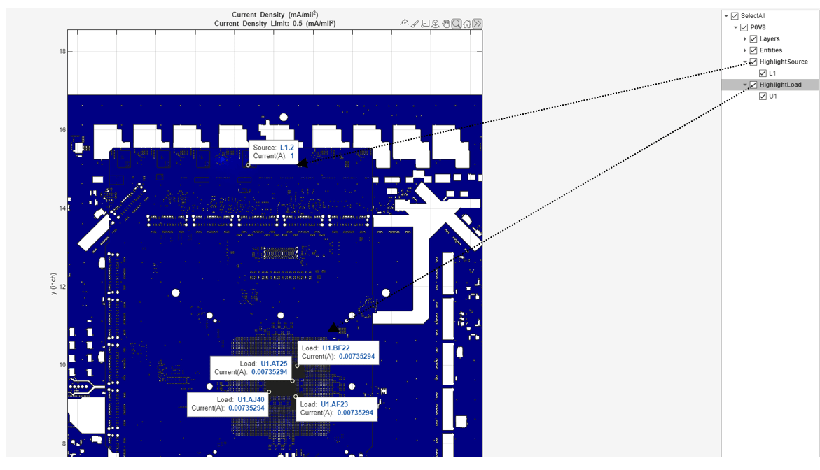
It is observed that the total current at the source is calculated as 1 A, which matches the load current specified earlier using setDCParameters.Each load pin of the ASIC (component U1) draws approximately 0.0073 A. There are 135 load pins of U1 connected to the 'P0V8' cadnet. The total current drawn by all load pins is 0.9855A which is very close to the expected 1 A. This analysis could further be extended by setting more than one source and confirming that the current is correctly distributed across the load pins and that the PDN model accurately reflects the system's electrical behavior.
Conclusion
This example demonstrates DC Power Integrity (PI-DC) analysis workflow for the P0V8 power net on a PCIe 5.0 Allegro board using MATLAB. The analysis validated the Power Delivery Network (PDN) design by ensuring that voltage levels across all load pins remained within acceptable limits and that current distribution was balanced, avoiding over-stress on any single path. Moreover, this methodology is scalable and can be extended to other power nets or more complex scenarios, such as multi-source configurations, to ensure uniform voltage and proper current sharing across all load pins.