Target QPSK Transmitter and Receiver to USRP E3xx Using HW/SW Co-Design Workflow
This example shows how to implement wireless communication algorithms on the USRP™ embedded series radio platform that are partitioned across the ARM® processing system and the FPGA programmable logic. This example is designed for a QPSK-based communication system.
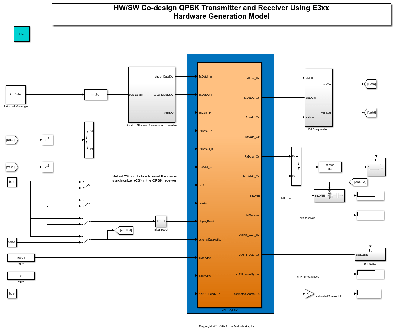
The following block diagram describes the hardware-software partitioning of the system and the implemented user logic.

Setup
To work with the HW/SW co-design workflow, you must install and configure additional support packages and third-party tools. For more information, see Installation for Hardware-Software Co-Design.
Hardware Generation Model
You need a hardware generation model to implement any design that runs on the programmable logic (PL). The HDL-optimized QPSK transmitter and receiver in the HDL QPSK Transmitter and Receiver example are used to implement the hardware generation model. This hardware generation model runs at single clock rate. Generate an HDL code for the hardware generation model and generate a software interface model template using HDL Workflow Advisor. Using the software interface model template, develop an interface model that runs on the processing system (PS).

Hardware-Software Partitioning
In general, the high rate signal processing is used for the programmable logic and the slower rate is used on the ARM. The user logic in FPGA programmable logic implements high rate processing modules, an ASCII to bit converter, a QPSK transmitter design, a channel, a QPSK receiver design, a bit to ASCII converter, and a compute BER module. Some control parameters and monitor signals are added to the FPGA IP core to adjust the design in real time and see the status of FPGA signals using AXI-Lite registers accessed from Simulink® via processing system. The ARM processing system pulls the status signals information from the FPGA and displays the information on the host.
To implement the FPGA IP core on the hardware platform, use IP Core Generation workflow with the following specific requirements.
HDL_QPSKsubsystem is the device under test (DUT) for the workflow. The DUT subsystem ports does not support complex data, so model real and imaginary signals at subsystem boundaries.Model data input and output ports using separate data and valid signals. The input and output clock rates of the DUT subsystem must be equal.
AXI4-lite ports: The externalDataActive input port switches messages from internal LUT (Hello World messages) to external message (USRP radio HW/SW Co-design QPSK). The overAir input port switches the data flow over the air to a loopback between QPSK Tx and QPSK Rx via a channel inside the FPGA. The insert CFO and insert CPO input ports sets the value of carrier frequency offset (CFO) and carrier phase offset (CPO) to be introduced to the waveform in the channel. The rstCS input port resets the carrier synchronizer in the QPSK receiver. The bitErrors and bitReceived ports streams the number of bit errors and number of bits received from the QPSK receiver. The numOfFramesSynced and estimatedCoarseCFO ports streams out the number of frames synchronized and the estimated coarse CFO.
Generate IP Core
If the simulation behavior of the hardware subsystem is as expected, you can start the process of generating the HDL IP Core, integrating it with the SDR reference design and generating software to run on the ARM.
In preparation for targeting, you must set up the Xilinx® tool chain by invoking hdlsetuptoolpath. For example:
>> hdlsetuptoolpath('ToolName','Xilinx Vivado','ToolPath','C:\Xilinx\Vivado\2019.1\bin\vivado.bat');
To generate the HDL IP core, right-click the HDL_QPSK subsystem and select HDL Code > HDL Workflow Advisor.
Expand 1. Set Target and click 1.1. Set Target Device and Synthesis Tool. In the right pane, set Target workflow to
IP Core Generationand Target platform toE310.
Click 1.2. Set Target Reference Design. In the right pane, set Reference design* to
Receive and Transmit path. For this example, use the default settings in the Reference design parameters pane.
Click 1.3. Set Target Interface. In the right pane, under the Target platform interface table pane map the DUT signals to the interface signals available in the reference design. Because this example uses a single channel, configure the channel 1 connections and AXI register interfaces as shown in these figures.


Click 1.4. Set Target Frequency. In the right pane, set Target Frequency (MHz) to
30.72. For this example, use the default settings in the Set Target Frequency pane.
Click 2. Prepare Model for HDL Code Generation. In the right pane, click Run All. The app prepares the model for HDL code generation by performing design checks.
Click 3. HDL Code Generation. In the right pane, click Run All. The app generates HDL code for the IP core.
Next, continue to use the HDL Workflow Advisor to generate the software interface model and block library.
Generate Software Interface Model and Block Library
Expand 4. Embedded System Integration. This step integrates the newly generated IP core project into the Zynq SDR reference design, generates the corresponding bitstream, and loads the bitstream onto the board.
Click 4.1. Create Project. In the right pane, click Run This Task. The app creates a project for the embedded system tool.
Click 4.2. Generate Software Interface Model. In the right pane, click Run This Task. The app generates a software interface library and a software interface model template.

The library contains the AXI Interface block generated from the HDL_QPSK subsystem. This block exposes only the AXI-lite control ports but not the data ports. The data ports are present on the transmitter and receiver blocks corresponding to your hardware selected in 1.1. Set Target Device and Synthesis Tool. The data ports of the transmitter and receiver blocks represent the streaming data interface between the FPGA user logic and ARM processor.
When using the library blocks in a downstream model, you must configure the parameters correctly for your application. Take into account that any updates to the HDL_QPSK subsystem are automatically propagated from the library blocks in the downstream model when you run 4.2. Generate Software Interface Model again.
Software Interface Model Template

Use the software interface model as a starting point for SW targeting to the Zynq: external mode simulation, processor-in-the-loop, or full deployment. Running the step 4.2 Generate Software Interface model overwrites the software interface model. So, it is suggested to save the model with a unique name and develop your software algorithm. A software interface model is provided with this example that shows how to structure this model.
Generate and Load Bitstream
The final steps of the HDL Workflow Advisor generate a bitstream for the PL and download the bitstream onto the board.
Click 4.3. Build FPGA Bitstream. In the right pane, click Run This Task. The app generates a bitstream for the PL. You can execute this step in an external shell by selecting Run build process externally. This selection allows you to continue using MATLAB® while building the FPGA image. After the basic project checks complete, the app marks this check with a green checkmark. However, you must wait until the external shell displays a successful bitstream build before moving on to the next step.
Click 4.4. Program Target Device. In the right pane, click Run This Task. The app downloads the bitstream onto the device. Before continuing with this step, call the zynq function to ensure that MATLAB has the correct physical IP address for the radio hardware:
>> devzynq = zynq('linux','192.168.3.2','root','root','/tmp');
By default, the physical IP address of the radio hardware is 192.168.3.2. If you alter the radio hardware IP address during the hardware setup process, you must supply that address instead.
Alternatively, if you want to load the bitstream outside the HDL Workflow Advisor, create a SDR radio object by using sdrdev object and use the downloadImage function.
>> radio = sdrdev('E3xx');
Download the bitstream using the radio object interfacing the selected radio device.
>> downloadImage(radio,'FPGAImage', ...
     'hdl_prj\vivado_ip_prj\vivado_prj.runs\impl_1\system_top.bit')
     % Path to the generated bitstream
Construct Software Interface Model
A software interface model is provided in this example that shows how to construct the generated model. You can run this interface model in monitor and tune mode or full deployed mode.
Note that in the software interface model, the E3xx Transmitter block handles the frame to sample serialization.

Set Up Software Model to run on ARM Processor
Set up the application model by following the guidelines in the Hardware-Software Co-Design Workflow, section Configure Software Interface Model. Configure the model to run using the Target Board Xilinx Zynq-7000 Based IIO Radio. To ensure efficient use of the ARM processor, the input size of the AD936x Transmitter block is set to nearly 10000 by concatenating external message multiple times and repeating each character by 16 times. As the message rate is 1/16th of the baseband sample rate, repeating each message character by 16 times maintains the message at baseband sample rate.
Run Software and Hardware on the Zynq Board
You can control the setup from the Simulink model in Monitor & Tune mode. Toggle the switch linked to the externalDataActive port to switch sourcing data between the FPGA stored LUT message and the ARM-based external message after running the design.
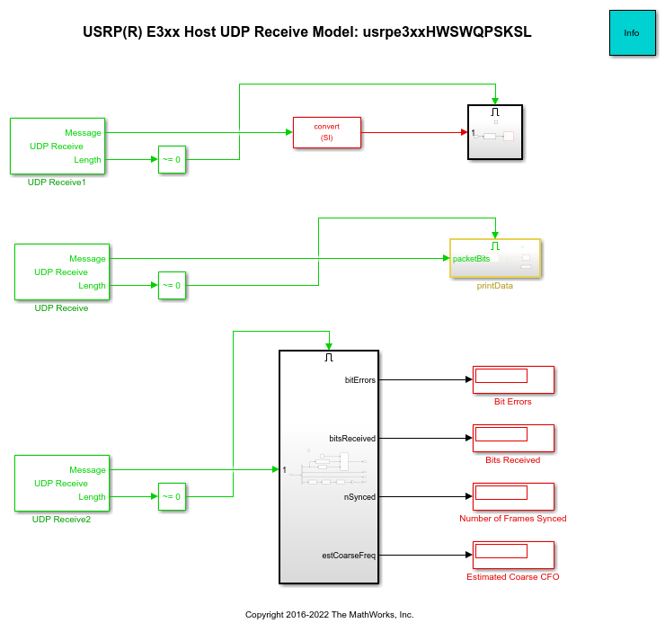
After the receiver decodes the message, the ARM processing system sends the result back to the host over the Ethernet link using the UDP send block found in the software interface model. The UDP send block is configured using the default IP address of the host '192.168.3.1'. If you altered the IP address during the hardware setup process, you must supply that address instead. A simple host UDP receive model is provided, which can be used to receive the decoded data and display the result in the diagnostic viewer.

You can also fully deploy the design to run on the board, disconnected from Simulink. In the Simulink toolbar, click Build, Deploy & Start. In this mode you cannot tune parameters.
Results
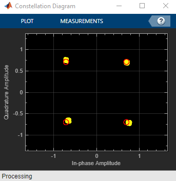
The following figures show the decoded message and constellations when the waveform is transmitted over the air. The diagnostic viewer displays the decoded message.
Constellation Plot

Host UDP Model - Internal LUT Message:

Host UDP Model - External Message:
