AXI4 Video Frame
        Buffer
R2026bModel connection between two hardware algorithms through external memory
Since R2022b
AXI4 Video Frame Buffer block
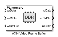
To add a block to a model, double-click the canvas and start typing the block name. Then, select the block from the list.
Libraries:
SoC Blockset for AMD /
SoC System Simulation /
Memory
HDL Coder /
SoC System Simulation /
Memory
Description
The AXI Video Frame Buffer block models a connection between two hardware algorithms through external memory, using full video frame buffers. The protocol is the MathWorks® streaming pixel protocol with back pressure. Also, the reader can ensure that the frame buffer is synchronized with downstream video timings by asserting an FSYNC protocol signal. The datapath includes a Video-DMA (VDMA) engine and the external memory buffers are managed as a circular buffer of full video frames.
This block is equivalent to a Memory Channel block with the
Channel type parameter set to AXI4 Video Frame
Buffer connected to a Memory Controller block.
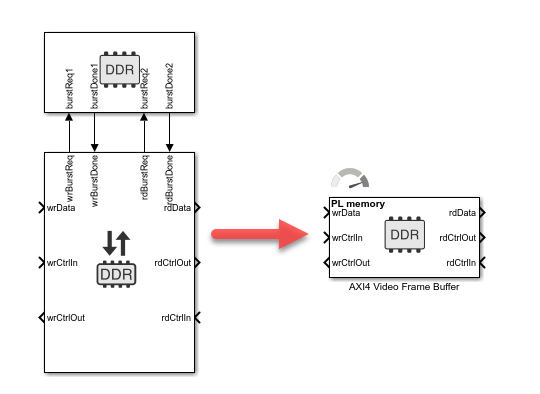
Since the memory controller is implicit to the design - you can instantiate several memory blocks that connect to the same memory unit via a memory controller. Valid blocks are:
AXI4 Random Access Memory (SoC Blockset)
AXI4-Stream to Software (SoC Blockset)
Software to AXI4-Stream (SoC Blockset)
AXI4 Video Frame Buffer (SoC Blockset)
Memory Traffic Generator (SoC Blockset)
The maximum number of manager interfaces in a model is 16.
For more information, see AXI4-Stream Video Interface (SoC Blockset).
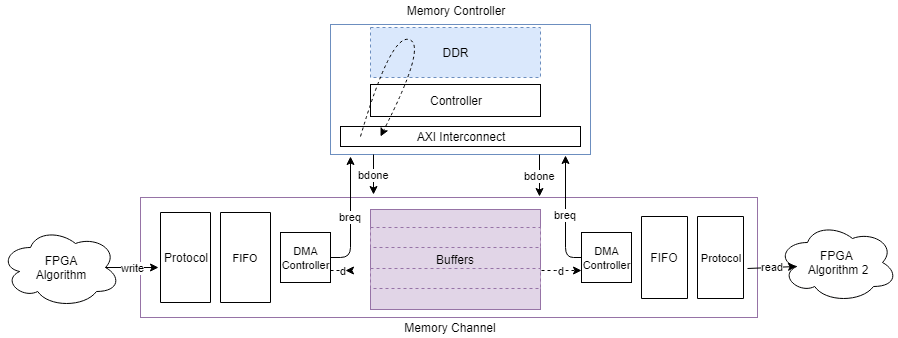
This image is a conceptual view of this block, streaming data from one FPGA algorithm to another FPGA algorithm.
Examples
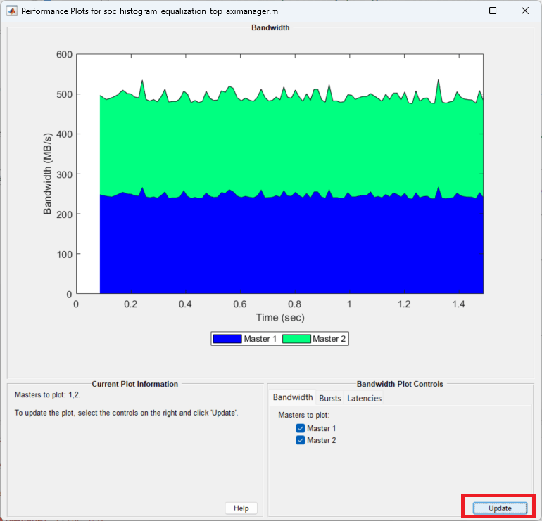
Histogram Equalization Using Video Frame Buffer
Perform histogram equalization with HDMI input and output and using external memory for video frame buffering.
Ports
Input
Output
Parameters
Memory simulation provides three levels of timing resolution. Select one of these options:
Burst accurate — Simulates memory contention and high-resolution timing.
Protocol accurate — Simulates AXI4 protocol hand-shaking sequencing and low-resolution timing.
Behavioral — Simulates data transactions only and no timing.
Tip
To enable performance logging, set this parameter to Burst
accurate. Use the Performance
Report (SoC Blockset) to display performance metrics.
Main
Select between processing subsystem (PS) or programming logic (PL) memory.
If the selected board supports only PL memory, then the default value is
PL memory.If the selected board supports only PS memory or only PL memory, then this parameter is read-only.
If the selected board is not a supported SoC board, then this parameter is not visible.
This parameter is read-only.
The size of the region in bytes. This value is calculated as the number of frames multiplied by the frame size multiplied by the size of the data. Define this value by setting the Frame size and Number of Frames parameters on the Main tab, and the Data type and Dimensions parameters on the Signal Attributes tab.
Example: A software frame size of 1024 uint32 defines a buffer of 4096 bytes. If the number of buffers is set to 2, the region size is 8192 bytes.
Select or enter the frame size in a combo box.
Select a frame format from the list or enter frame dimension as a 2 element vector
such as [1920 1080].
480p SDTV (720x480p)576p SDTV (720x576p)720p HDTV (1280x720p)1080p HDTV (1920x1080p)160x120p320x240p640x480p800x600p1024x768p1280x768p1280x1024p1360x768p1400x1050p1600x1200p1680x1050p1920x1200p
Define the number of video frames in the memory.
The memory access has a ring-buffer pattern. The writer can continually write as long as buffers are available. When a buffer is completed, it becomes available for the reader. The writer and reader traverse the buffers in a circular pattern. As long as the writer and reader maintain similar rates, the buffering prevents blockage.
A disparate rate between a reader and a writer slows down the faster device. For example, a slow reader causes the writer to run out of buffers and blocks the writer, effectively slowing down the writer to the reader rate. Likewise, a slow writer causes the reader to run out of buffers and blocks the reader, effectively slowing down the reader to the writer rate.
The Number of Frames parameter must be an integer from 3 to 64.
The length of bursts for this connection on the memory bus in units of scalar data. The scalar unit is the packed data type. Specify the burst size for both writer and reader access to the channel.
The channel data is always transferred to the memory model using burst transactions. For the AXI4 configuration, the algorithm logic is responsible for defining the burst through the protocol signals.
The Burst length parameter determines the burst size to the memory, and the rdData signal defines the size of each transfer on the interface.
Specify the depth of the data FIFO, in units of bursts. When the writer has no buffers to write to, the FIFO can absorb data until a buffer becomes available. This value is the maximum number of bursts that the FIFO can buffer before it drops data.
Dependencies
To enable this parameter, select Burst accurate under Memory simulation.
Specify a number that asserts a backpressure signal from the channel to the data source. To avoid dropping data, set a high watermark, allowing the data producer enough time to react to backpressure. This number must be smaller than the FIFO depth.
Dependencies
To enable this parameter, select Burst accurate under Memory simulation.
Specify the frequency of the manager datapath in MHz.
Dependencies
To enable this parameter, select Burst accurate under Memory simulation.
Specify the data width of the manager datapath to the interconnect controller in bits.
Dependencies
To enable this parameter, select Burst accurate under Memory simulation.
Signal Attributes
Data signal
Specify the dimension for the video data as a whole scalar or vector.
Example: [1 3] — A pixel represented by three values (for red,
green, and blue).
Example: [1080 1920 3] — A 1080p frame. The frame includes 1080
lines of 1920 pixels per line, and each pixel is represented by three values (for red,
green, and blue).
Specify the data type of the video pixel. For help, click the ... button and select Data Type Assistant. By default, this value is set to inherit the data type from the source signal.
Specify a time interval in seconds to define how often the block updates.
When you do not want the output to have a time offset, specify the
Sample time parameter as a scalar. To add a time offset to the
output, specify the Sample time parameter as a
1-by-2 vector, where the first element is the
sampling period and the second element is the offset. For more information about
sample times in Simulink®, see Specify Sample Time.
Select this parameter to enable data packing across the last dimension of the
signal. For example, if the channel data type is uint32, the
dimensions are [1024 4]. If you select this sample packing
parameter, then the memory channel generates 1024 read or write transactions of 128
bits. If you clear this sample packing parameter, the memory channel generates 4096
transactions of 32 bits each.
This figure shows how data is aligned for a signal with data type
fixdt10[4x3]. When the data is packed, three 10-bit words are
concatenated and extended by 2 bits to a 32-bit word. When the data is not packed,
each 10-bit word is extended to a 16-bit word.

This figure shows how data is aligned for a signal with data type
uint8[8x3]. When the data is packed, three 8-bit words are
concatenated and extended by 8 bits to a 32-bit word. When the data is not packed,
each 8-bit word is represented as an 8-bit sample.

The combined width of the flattened signal must not exceed 512 bits.
Select this box to make the reader inherit the sample time offset from the writer. Clear the box to use a different sample time offset from the writer. For more information about sample time offsets, see Sample Time Offset.
Select this box to use the pixel clock sample time. To use the pixel clock sample time, you must use scalar pixel dimensions. The pixel clock sample time is relevant only when streaming pixels. If both the reader and the writer are streaming frames, you get an error when checking this box.
Extended Capabilities
Version History
Introduced in R2022bSee Also
AXI4 Random Access Memory (SoC Blockset) | AXI4-Stream to Software (SoC Blockset) | Software to AXI4-Stream (SoC Blockset)
Topics
- External Memory Channel Protocols (SoC Blockset)

