Buck Power Train Design Workflow
This example shows how to use the MathWorks® switched mode power supply (SMPS) workflow to design a power supply with a buck power train.
The buck power train circuit topology is one of the most basic SMPS power train topologies, used to convert an input DC voltage to a lower DC output voltage with the same polarity. You can use the MathWorks SMPS workflow to design the buck power train for a specified operating point or range of operating points, design a proportional-integral-derivative (PID) compensator to control the output voltage, and simulate the power supply's behavior in dynamic conditions.
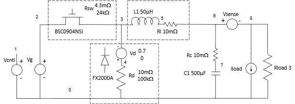
This example uses the buck power train circuit shown in the schematic diagram below and described in the netlist file BuckPowerTrain.sp.
Operating Point Analysis
You can use operating point analysis to design the power train and analyze its performance under steady state operating conditions. For more information, see Boost Power Train Operating Point Analysis.
If you use the configuration file BuckPowerTrain_Cfg1 included with this example to configure and run the operating point analysis, you will obtain the data contained in the file BuckPowerTrain_Cfg1Out. The DcResults table in this file also contains the metrics added through the post-processing script getPowerTrainMetrics included as part of the operating point analysis example.
DC Results Table
load('BuckPowerTrain_Cfg1Out.mat');
BuckPowerTrain_Cfg1Out.DcResults(:,1:7)
ans =

  1×7 table

    Duty Cycle    Frequency    Vg    Iload    Vout    Iout      Ig
    __________    _________    __    _____    ____    ____    _______

     0.55245        1e+05      28      0       15      5      -2.7626
Power Analysis Table
BuckPowerTrain_Cfg1Out.DcResults(:,8:18)
ans =

  1×11 table

    P_Vcntl     P_Vg       P_Rsw      P_Vd      P_Rd       P_Rl        P_Rc       P_Vsense    P_Rload    P_Iload    P_total
    _______    _______    _______    ______    _______    _______    _________    ________    _______    _______    ________

       0       -77.296    0.43242    1.5681    0.11701    0.25173    0.0016496       0          75          0       0.075021
Efficiency and Ripple Metrics
BuckPowerTrain_Cfg1Out.DcResults(:,19:end)
ans =

  1×5 table

    Efficiency    Vin_ripple    Iin_ripple    Vout_ripple    Iout_ripple
    __________    __________    __________    ___________    ___________

      0.9703          0           5.7074       0.014105       0.0047018
The Waves table in the BuckPowerTrain_Cfg1Out file provides access to all of the steady state voltage and current waveforms in the power train circuit, and you can use these waveforms to gain insights into the way the circuit operates. For example, the waveform at the switching node (node 3) of the circuit demonstrates the effect of the switching device and diode on the input voltage of the inductor. When the switching device is turned on, it draws current from the input supply, through the inductor and into the decoupling capacitor and load. During this period, the switching node is at a higher voltage than the output, causing the current in the inductor to increase. However when the switching device is turned off, the only current path available to the inductor is the diode to the return node. Since the current must continue to flow, the inductor drives the diode's negative terminal below the return voltage. This causes the inductor current to decrease, but it continues to flow unless/until the current in the diode reaches zero, turning the diode off.
Switching Node Waveforms
t       = BuckPowerTrain_Cfg1Out.Waves{1}.Time;
vswitch = BuckPowerTrain_Cfg1Out.Waves{1}.('3');
iL1     = BuckPowerTrain_Cfg1Out.Waves{1}.iL1;
figure(1);
tiledlayout(2,1);
% Inductor output voltage
nexttile;
plot(t,vswitch);
title('Buck Power Train Switching Node Waveform');
% Inductor current
nexttile;
plot(t,iL1);
title('Buck Power Train Inductor Current');
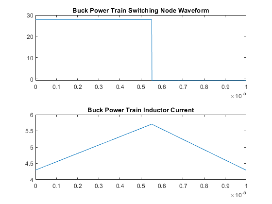
From the operating point analysis and the configuration file BuckPowerTrain_Cfg1 you can also build a Simulink® block that can be used to model the power train in a time domain simulation ("Build block" from the Linear Circuit Wizard mask). The Power Train block in the BuckPowerSupply Simulink model was constructed this way.
Compensator Design
Reference [1] explains how to design a PID controller to control a buck power train. The PID compensator circuit shown in the schematic below and described in the file PIDCompensator.sp was designed using the method given in [1].
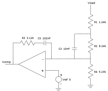
You can obtain the poles, zeros and symbolic model of this circuit and optimize its design by applying the configuration in the file PIDCompensator_Cfg1 to the method described in the Feedback Amplifier Design for Voltage-Mode Boost Converter example. You can find the results obtained for the starting configuration in the file PIDCompensator_Cfg1Out attached to this example.
load('PIDCompensator_Cfg1Out.mat');
PIDCompensator_Cfg1PoleZero
PIDCompensator_Cfg1SymbolicModel
PIDCompensator_Cfg1PoleZero =

  struct with fields:

              Poles: [2×1 double]
              Zeros: {[2×1 double]  [2×1 double]}
              Gains: [-329.5526 1.0000e+03]
     InputPortNames: {'Vload'  'Vref'}
    OutputPortNames: {'Vcomp'}


PIDCompensator_Cfg1SymbolicModel =

  struct with fields:

      As: {2×2 cell}
      Bs: {2×2 cell}
      Cs: {1×2 cell}
      Ds: {'-333.3333*R1^-1'  '333.3333*R1^-1'}
    e11s: {'3e-08*C3'}
    f22s: {'333.6667*R3^-1 + 0.33333*R4^-1 + 0.33333*R1^-1'}
You can also build a Simulink block for the compensator, either from the configuration in PIDCompensator_Cfg1 or for an optimized compensator that you have designed ("Build block" from the Linear Circuit Wizard mask). The Compensator block in the BuckPowerSupply Simulink model was constructed this way.
Time Domain Simulation
You can combine the power train Simulink block from the operating point analysis with the compensator Simulink block from the controller design and a pulse width modulator (PWM) to be discussed in this section to create a time domain simulation of the closed loop behavior of the power supply.
The PWM interacts with ripple at the output of the compensator, making details of the PWM design/definition important. While most analyses ignore any ripple that passes from the output of the power train to the output of the compensator, there can be ripple at the output of the compensator that significantly affects the closed loop behavior of the power supply. Power train output ripple is inherently synchronous with the control signal provided by the PWM, and so any delay between the time the PWM derives the width of the next pulse from the compensator output and the time the PWM outputs that pulse will increase the delay in the control loop and reduce the phase margin. Ripple at the compensator output also appears to affect the small signal behavior of the control loop in other ways that should be evaluated through analysis of time domain simulation results.
The model BuckPowerSupply enables you to switch between two different PWMs.
open('BuckPowerSupply.slx');
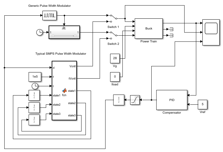
The first choice offered is the Simulink PWM block, which reads the output pulse width from the control input on the rising edge of the output pulse. To use this PWM, set the manual switches Switch 1 and Switch 2 in the model to their upper positions. Run this model and compare the steady state outputs of the power train output and the compensator to the output of the PWM. Note that the steady state duty cycle of 0.5524 occurs near the beginning of the ripple cycle and that the ripple voltage increases from there.
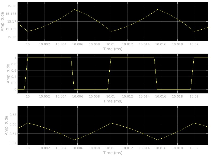
Many texts on SMPS specify the PWM circuit shown below explicitly and in detail for voltage controlled operation. Note that in this circuit the falling edge of the PWM output occurs essentially as soon as the sawtooth ramp has become higher than the compensator output.

The other PWM choice in the model BuckPowerSupply uses a MATLAB® function block and several unit delay blocks to closely approximate the behavior of this circuit. To use this PWM, set the manual switches Switch 1 and Switch 2 in the model to their lower positions. Run BuckPowerSupply and note that the falling edge of the PWM output occurs at the peak of the compensator output ripple waveform, and that the value at that point is equal to the steady state output duty cycle.

References
1. R. W. Erickson and D. Maksimovic, Fundementals of Power Electronics, 3rd, Ed., Cham, Switzerland: Springer Nature, 2020.