Convert to and from Simulink Signals
Signal Conversion Specifications
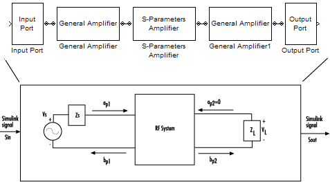
When you simulate an RF model, the blockset must convert the mathematical Simulink® signals to and from the physical modeling environment. The following figure shows the signals involved in the conversion.

Where:
ZS is the Source impedance (ohms) parameter of the Input Port block.
ZL is the Load impedance (ohms) parameter of the Output Port block.
There are two options for interpreting the Simulink signal that enters the Input Port block:
Sin is the incident power wave. For more information about this option, see Interpret Simulink Signals as Incident Power Waves.
Sin is the source voltage. For more information about this option, see Interpret Simulink Signals as Source Voltages.
Interpret Simulink Signals as Incident Power Waves
The blockset provides the option to interpret the input Simulink signal, Sin, as the incident power wave, ap1, at the first port of the RF system. The following figure shows the model for this interpretation.

In the figure, bp2 is the transmitted power wave at the second port of the RF system. This is the signal at the output of the Output Port block, Sout.
For a 2-port RF system, the incident and transmitted power waves are defined as:
where:
ZS, the Source impedance (ohms) parameter of the Input Port block, is defined as:
ZS = RS + jXS
ZL, the Load impedance (ohms) parameter of the Output Port block, is defined as:
ZL = RL + jXL
Solving the power wave equations for Sin and Sout gives the following relationships:
The implications of this interpretation are:
is equal to the power available from the source, Pavs.
is equal to the power delivered to the load, Pout.
For a linear RF system, where Gt is the transducer power gain. As a result, the Simulink signals at the input and output of the RF system have the following relationship:
Note
You can plot Gt from the Output Port block's Visualization tab.
Interpret Simulink Signals as Source Voltages
The blockset provides the option to interpret the input Simulink signal, Sin, as the source voltage, VS, of the RF system. The following figure shows the model for this interpretation.

With this interpretation, the signal at the output of the Output Port block is the load voltage, VL.
The blockset interpretation of the input Simulink signal as the source voltage, VS, produces different results than the interpretation where the input Simulink signal is the incident power wave. When the source and load impedances are the same and real, the former interpretation produces 6 dB of loss compared to the latter.
Specify Input Signal Conversions
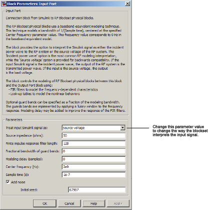
To specify the way in which the blockset interprets the input Simulink signal, you change the value of the Treat input Simulink signal as parameter in the Input Port dialog box. The available parameter values are:
Incident power wave— Interpret the input signal as the incident power wave.Source voltage— Interpret the input signal as the source voltage.

See Also
General Amplifier | Input Port | Output Port | S-Parameters Amplifier