Design Optimization Using Frequency-Domain Check Blocks (GUI)
This example shows how to optimize model parameters to meet frequency-domain requirements using the Response Optimizer. Simulink® Control Design™ software must be installed to optimize a design to meet frequency-domain design requirements.
In this example, you specify the design requirements in a Bode Plot, Check Bode Characteristics (Simulink Control Design) block. You optimize rectifier filter parameters to meet gain and bandwidth requirements by minimizing a custom objective.
Full Wave Rectifier Model
Open the model.
open_system('sdorectifier.slx')Model Structure
The model sdorectifier includes the following blocks:

Full-Wave Rectifier block — An Abs block
Rectifier Filter subsystem — RLC filter implemented using integrator and gain blocks
Filter Design Requirements block — Bode Plot, Check Bode Characteristics (Simulink Control Design) block that specifies the gain and bandwidth design requirements
Design Requirements
The design optimization problem has several objectives. The design must:
Have a –3 dB bandwidth of at least 2 Hz
Limit the gain across the frequency range 2 Hz – 60 Hz to at most 0 dB
Limit the gain above 60 Hz to at most –20 dB
Maximize the filter resistance R
Minimize the filter inductance L
The requirements ensure that the rectifier filter combination has minimal high frequency content, responds quickly to voltage changes, and limits filter currents.
Specify Design Requirements
To open the app, in the Apps gallery, click Response Optimizer.

The Bode plot 1 tab shows the gain and bandwidth requirements specified in the Filter Design Requirements block in the model. To see their values, double-click the block to open the Block Parameters dialog box, and select the Bounds tab.
Specify a custom objective to minimize the filter inductance and maximize the resistance.
The custom objective is already defined in the
sdorectifier_costfunction. The function accepts the design variables R and L and returns the objective to be minimized.Tip
Type
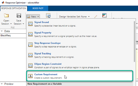
edit sdorectifier_costin the command line to view this function.In the New drop-down list, select Custom Requirement.

Specify the following values in the Create Requirement window, and click OK:
In the Name edit box, enter
MaxMinRL.In the Type edit box, select
Minimize the function
            output
In the Function edit box, enter
@sdorectifier_cost. The optimization solver calls the specified function handle.

A new requirement variable
MaxMinRLis created, and appears in the Data area in the Response Optimizer. The Iteration plot 1 tab shows the value ofMaxMinRLat each iteration during the optimization.
Specify Design Variables
When you optimize the model response, the software modifies the design variable values to meet the design requirements.
In the Design Variables Set drop-down list, select New.

Select
C,L, and R in the Create Design Variable Set window. Click to add the selected parameters to a design variables
set.
Specify the value range for each design variable, and click OK:
Cin the range 1 µF–1 mFLin the range 1–500 mHRin the range 0.01–50 ohms
A new variable
DesignVarsis created, and appears in the Data area of the Response Optimizer.
Optimize Design
To view the current response of the model, click
 Plot Model Response.
The Bode plot 1 window in the Response Optimizer shows that the model output goes out of the region bounded by the design requirement line segments.
In the
Voltagescope window, you see that the filter voltage signal overshoots its steady-state value and contains significant harmonic content.
Click
 Optimize.
The
Optimization convergedmessage in the Optimization Progress Report indicates that the optimization method found a solution to satisfy the filter bandwidth requirements.
The harmonic content in the filter voltage signal is reduced from the initial design.

Verify that the model meets the gain and bandwidth requirements.

The plot displays the output of the last five iterations. The final response using the optimized parameter values appears as the thick blue line.
The optimized response lies in the white region bounded by the design requirement line segments and thus meets the requirements.
Click
DesignVarsin the Data area and view the updated values in the Variable Preview area.The optimized values of the design variables are automatically updated in the Simulink model.
See Also
Bode Plot, Check Bode Characteristics (Simulink Control Design)