LTE SIB1 Recovery Using Analog Devices AD9361/AD9364
This example implements a receiver system to recover the first system information block (SIB1) from an LTE downlink signal using a Xilinx (TM) Zynq radio platform that is partitioned across the ARM and the programmable logic (PL) fabric.
Limitations:
Due to limited hardware resources, this example does not support
ZedBoard and FMCOMMS2/3/4.Due to the size and complexity of this example, it can take a long time to simulate.
Due to the size and complexity of this example, it can take a long time for HDL code and bitstream generation.
Introduction
The LTE HDL SIB1 Recovery (Wireless HDL Toolbox) model is a hardware friendly model. You can use this model to detect the SIB1 information from synthesized data generated by the LTE Toolbox or captured off-the-air LTE waveforms. This example shows how to adapt the model to software-defined radio (SDR) hardware, and how to prototype it on the Zynq platform. A system will be developed to receive SIB1 information at a single center frequency.
Setup
If you have not already done so, ensure you follow the Installation for Hardware-Software Co-Design in the documentation.
Hardware Generation Model
The hardware generation model is used to develop the functionality that you wish to implement on the FPGA fabric. In this example, we implement a SIB1 recovery receiver based on the LTE HDL SIB1 Recovery (Wireless HDL Toolbox) example. The following figure shows the hardware architecture diagram of the SIB1 recovery example.

This Simulink model implements the architecture shown above. The algorithm is partitioned into Rx Hardware Algorithm and Rx Software Algorithm to run on ARM, as shown by the colored areas.
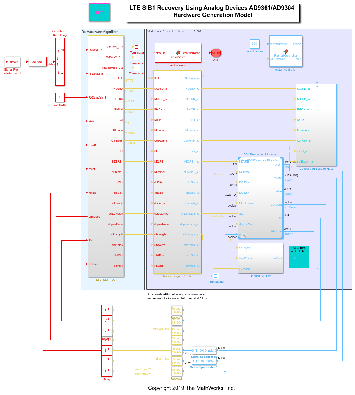
Hardware-software partitioning: In this example, the SIB1 recovery algorithm is implemented mostly in the FPGA, due to the high rate signal processing requirements of the design. The FPGA performs synchronization and demodulation of the received OFDM signal, channel estimation and equalization of the resource grid, as well as decoding of the following channels:
Physical broadcast channel (PBCH)
Physical control format indicator channel (PCFICH)
Physical downlink control channel (PDCCH)
Physical downlink shared channel (PDSCH)
The ARM parses the downlink control information (DCI) message then uses this information to perform the DCI physical resource block (PRB) allocation calculation. The PRBs are then communicated back to the PL, to decode the PDSCH, and the SIB1 message bits are returned. The ARM also pulls information from the FPGA, sends some useful information back to the host over UDP for display, and controls the start/reset of the FPGA IP. The LTE_SIB1_HDL subsystem contains the functionality to be implemented on the FPGA. Around this subsystem is the functionality that will eventually be implemented on the ARM processor on the Zynq hardware. In the hardware model, the communication back to the FPGA is replaced with a simple interface which displays the decoded information. The software can also control which input data to use: off-the-air or test data stored on the FPGA. To simulate software execution on hardware, the output data of the subsystem is downsampled by 1000.
The LTE SIB1 recovery subsystem is shown below.

In this subsystem, the HDL LTE SIB1 subsystem contains the cell search and SIB1 recovery algorithm, as presented in the LTE HDL SIB1 Recovery (Wireless HDL Toolbox) example.
Additionally, the SIB_Bit_Packing subsystem packs individual SIB1 message bits (if decoded) into a vector of 32 uint32 values to allow for efficient transfer between the PL and the ARM. The SIB_Bit_Packing subsystem also provides a sibLen value, that indicates the length of the SIB1 message in bits, and a sibWordCnt value, that indicates the number of elements in the 32-length vector which are populated by the SIB1 message. As the vector can hold a maximum of 32 uint32 values, the maximum length of SIB1 message that can be transferred between the PL and the ARM is 32x32 = 1024 bits.
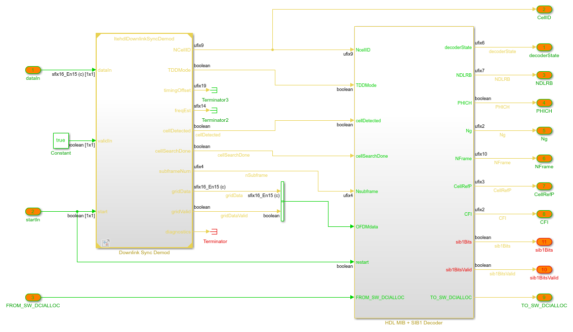
In addition to the algorithm, the subsystem also provides functionality for integration with the Zynq hardware architecture.
At the input to the HDL LTE SIB1 subsystem, some adjustments are made to the received data in the PrepInputs subsystem. The data from the AD9361 is a 12 bit number, sign extended to 16 bits. In order to use the full range the samples are scaled up to 16 bits. To take advantage of hardware resource sharing and simplify some of the architectures found in the receiver, the data rate into the system is configured to be higher than required. The input data rate is 61.44MHz, whereas the required maximum data rate is 30.72MHz. This difference translates to an overclocking factor of  . Therefore, upon entering the detector, the data is immediately downsampled by a factor of 2. An FIR Decimation block is used to implement a lowpass decimation filter which captures the central part of the received LTE waveform and downsamples the data to 30.72MHz.
You can run this model to confirm its operation using the captured LTE waveforms in zynqRadioLTETransmitData.mat. The test waveforms used in the model are configured in the initialization script. As the model contains a large number of HDL-optimized blocks, requiring simulation using sample-based signals, the simulation runs very slowly. When a SIB1 is decoded, the SIB1 GUI will pop up with the decoded information.
IP Core Generation Workflow
Once you are satisfied with the simulation behavior of the hardware subsystem, you can start the process of generating the HDL IP Core, integrating it with the SDR reference design, and generating software for the ARM processor.
In preparation for targeting, you must set up the Xilinx tool chain by invoking hdlsetuptoolpath. For example:
>> hdlsetuptoolpath('ToolName','Xilinx Vivado','ToolPath','C:\Xilinx\Vivado\2019.1\bin\vivado.bat');
Start the targeting workflow by right-clicking the LTE_SIB1_HDL subsystem and selecting HDL Code / HDL Workflow Advisor.
In Step 1.1, select
IP Core Generationworkflow and the appropriate Zynq radio platform. Choose either ADI RF SOM, ZC706 and FMCOMMS2/3/4, ZCU102 and FMCOMMS2/3/4, ZC706 and FMCOMMS5. Due to limited hardware resources, this example does not support ZedBoard and FMCOMMS2/3/4.
In Step 1.2, select
Receive pathreference design. You can leave the reference design parameters as the defaults.
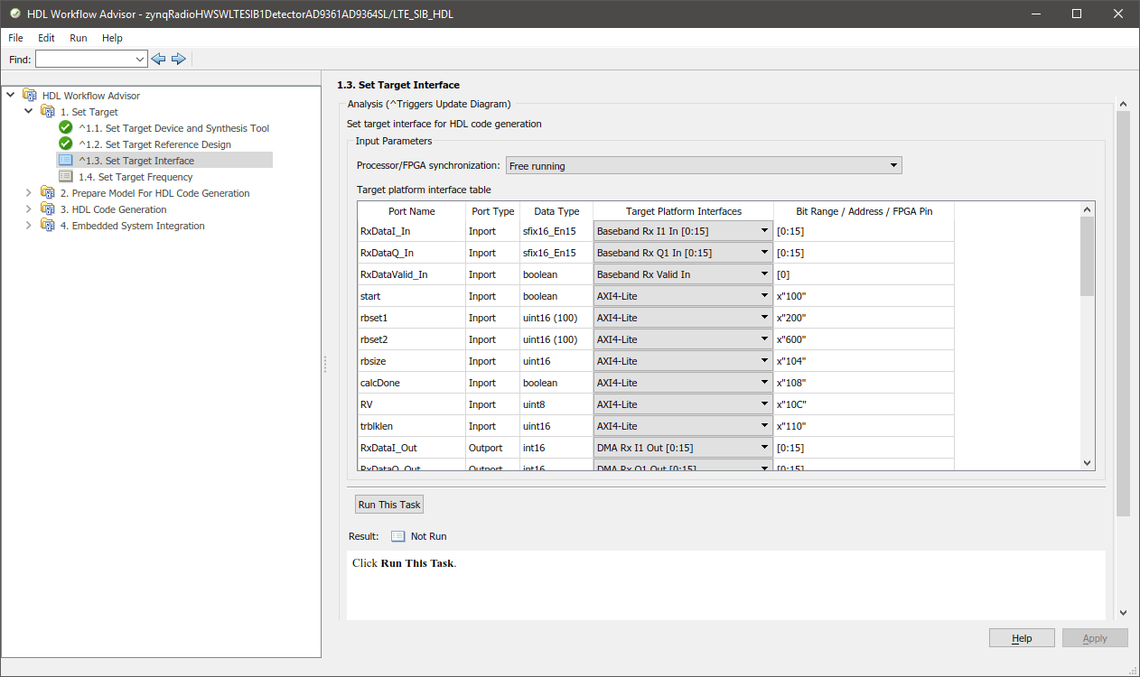
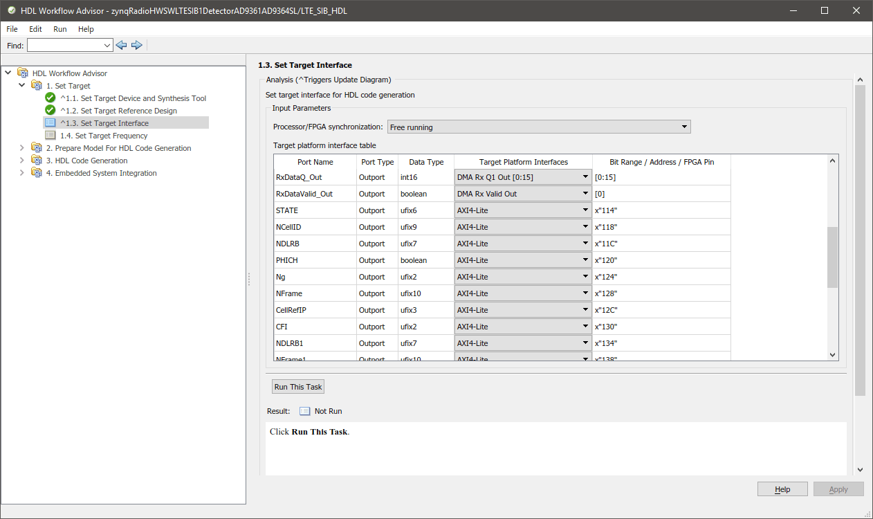
In Step 1.3, the interface table can be used to map the DUT signals to the interface signals available in the reference design. In this example, we only use a single channel, so the channel 1 connections and AXI register interfaces should be configured as shown in the three images below.

In Step 1.4, ensure that the Target Frequency is set to a reasonable number given the baseband sampling rate of the system. In this example, the sample rate is 61.44 MHz, so the maximum synthesis frequency of 61.44 MHz is required.
Step 2 prepares the design for code generation by doing some design checks.
Step 3 performs the actual HDL code generation for the IP core.
Step 4 integrates the newly generated IP core into the larger Zynq SDR reference design, generates the bitstream, and helps you load it onto the board.
Execute each step in sequence to experience the full workflow. Alternatively, if you are already familiar with the workflow, right click Step 4.1 in the table of contents on the left hand side and select Run to selected task. You can use the default settings in Steps 2 and 3, but for faster HDL code generation, set the 'Scalarize ports' option in step 3.1.3 to 'DUT level'.
Software Generation Model and Block Library
In Step 4.2, the workflow generates a Zynq software generation interface model and a block library. Click the
Run this taskbutton with the default settings.
Software Interface Library
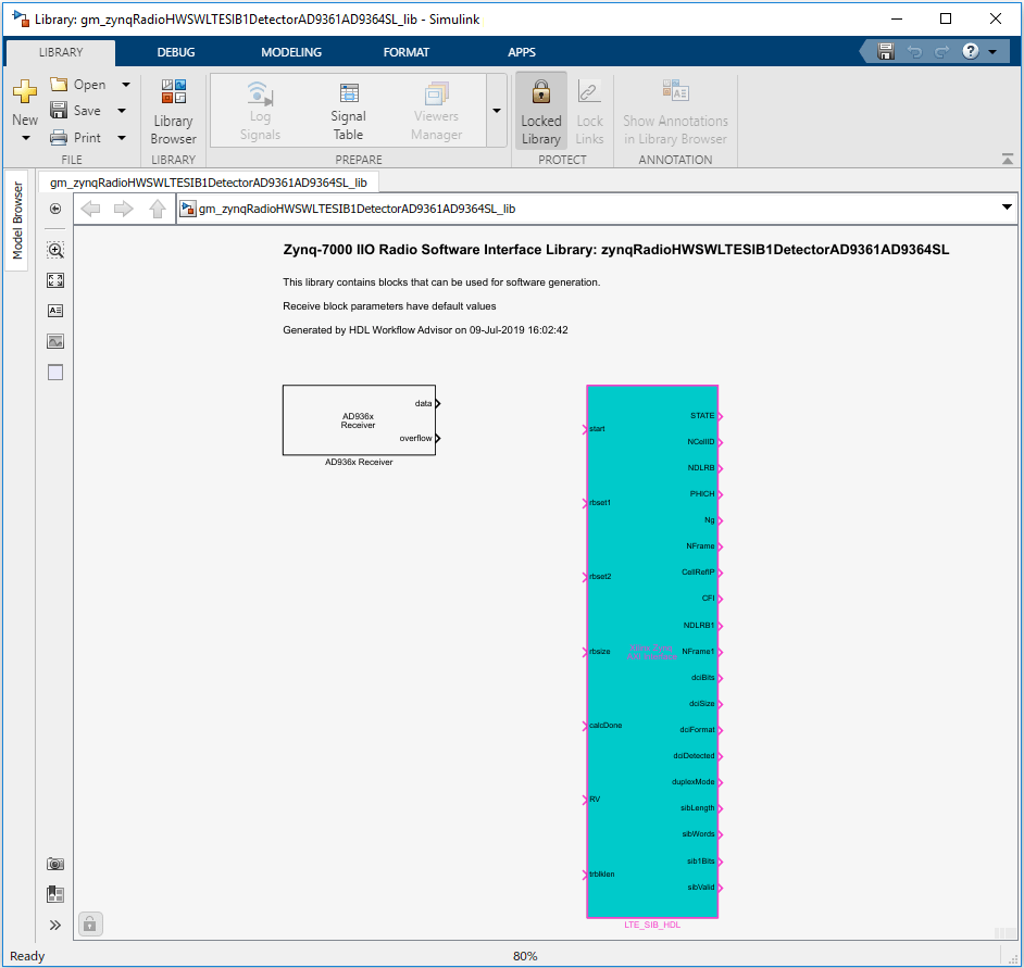
The library contains the AXI Interface block generated from the LTE_SIB1_HDL subsystem. The data ports present on the Receiver block represent the streaming data interface between the FPGA user logic and the ARM. If you use the library blocks in your downstream models, any updates to your HDL subsystem are automatically propagated to this library and to your software generation models. In this example, the hardware generation model did not contain SDR transmit or receive blocks, so the parameters on these blocks are populated with default values. When using the library blocks, you must configure the parameters correctly for your application.
Software Interface Model
You can use the generated software interface model as a starting point for full SW targeting to the Zynq: external mode simulation, processor-in-the-loop, and full deployment. Note that the generated model is overwritten each time you run Step 4.2. To further develop your software algorithm, save the model under a unique name. For a software interface model that shows how you can structure this model, see section Running the Software and Hardware on the Zynq board.
Bitstream Generation and Loading
Use the rest of the workflow to generate a bitstream for the FPGA fabric and to download the bitstream to the board.
In Step 4.3, the Workflow Advisor generates a bitstream for the FPGA fabric. You can choose to execute this step in an external shell by ticking the selection
Run build process externally. This selection allows you to continue using MATLAB while the FPGA image is being built. The step requires a couple of minutes to complete after some basic project checks. When a green checkmark indicates that the step is complete, you must still wait until the external shell shows a successful bitstream build before moving on to the next step.
Step 4.4 downloads the bitstream onto the device. Before continuing with this step, call the
zynqfunction with the following syntax to make sure that MATLAB is set up with the correct physical IP address of the radio hardware.
>> devzynq = zynq('linux','192.168.3.2','root','root','/tmp');
By default, the physical IP address of the radio hardware is 192.168.3.2. If you alter the radio hardware IP address during the hardware setup process, you must supply that address instead.
Alternatively, if you want to load the bitstream outside Workflow Advisor, create an SDR radio object and call the downloadImage function on the object.
If in Step 1.1 you selected either the ADI RF SOM, the ZC706 and FMCOMMS2/3/4, or the ZCU102 and FMCOMMS2/3/4 radio device, create an AD936x radio object.
>> radio = sdrdev('AD936x');
If in Step 1.1 you selected the ZC706 and FMCOMMS5 radio device, create an FMCOMMS5 radio object.
>> radio = sdrdev('FMCOMMS5');
Download the bitstream using the radio object.
>> downloadImage(radio,'FPGAImage', ...
     'hdl_prj\vivado_ip_prj\vivado_prj.runs\impl_1\system_top.bit')
     % Path to the generated bitstream
Running the Software and Hardware on the Zynq board
The following software interface model allows you to run the example system in Monitor & Tune or fully deployed.
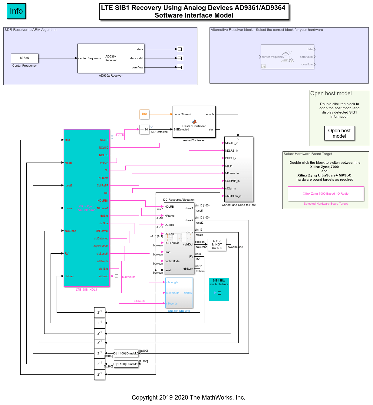
The software interface model was created from the generated software model in Step 4.2 of the HDL Workflow Advisor, and has been configured to run using the Xilinx Zynq-7000 Based Board target for the following hardware: ADI RF SOM ZC706 and FMCOMMS2/3/4/5
If you are using the ZCU102 and FMCOMMS2/3/4, double click the Selected Hardware Board Target block to change the configuration to use the Xilinx Zynq UltraScale+ MPSoC ZCU102 board target.
The model is configured to run on a timer interrupt. This means that the code generated from the Simulink model is executed on the ARM processor at a rate corresponding to the maximum rate in the software interface model. In this case, the model is configured to run at a rate of 1kHz, thus the AXI registers on the FPGA are read 1000 times per second.
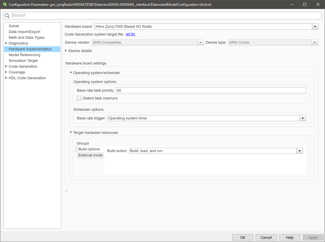
For more information on setting up the software interface model, refer to Hardware-Software Co-Design Workflow.
You can detect an LTE SIB1 by choosing the transmission center frequency of an LTE cell tower in your area. The default center frequency for this example is 806 MHz.
Monitor & Tune mode allows you to control the configuration from the Simulink model. You can also fully deploy the design to run on the board, disconnected from Simulink. In the Simulink toolbar, click Build, Deploy & Start.
The software algorithm is set up to reset the receiver on a timeout with default value 100 ms. The same value is configured for the hardware start signal.
The decoded SIB1 message bits are available at the output of the Unpack SIB1 Bits subsystem.
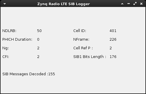
The ARM sends the decoded SIB1 information directly back to the host over the Ethernet link using the UDP send block. The UDP send block is configured using the default IP address of the host '192.168.3.1'. If you alter the IP addresses during the hardware setup process, you must supply that address instead. The following UDP receive model illustrates how to receive the decoded data, and displays the result.
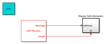
When running successfully, the host model displays the decoded cell information.
Using a generated Waveform
If you do not have access to an LTE signal, you can use the transmitRepeat function to transmit a generated LTE waveform.
load('eNodeBWaveform.mat');
tx = sdrtx('AD936x');
tx.BasebandSampleRate = 61.44e6;
tx.CenterFrequency = 806e6;
transmitRepeat(tx, resample(rxWaveform, 61.44e6, fs));
Troubleshooting
Some RF front-ends can have large frequency offsets which can make it hard to decode an LTE signal. The maximum offset that can be corrected is 7.5kHz. You can try the following techniques to identify a frequency offset.
If you have LTE Toolbox, you can run the LTE MIB Receiver script to look for LTE signals at chosen center frequencies. Edit the center frequency in the script to attempt to receive an LTE signal. The script will output the detected frequency offset on the command prompt.
You can add or subtract 3.75kHz from your chosen center frequency in the SIB1 Detector. If your offset is greater than 7.5kHz, you can progressively try higher or lower frequencies.
See Also
Functions
Blocks
Topics
- LTE HDL SIB1 Recovery (Wireless HDL Toolbox)