Model and Analyze Planar Photonic Band Gap Structure
This example shows how to create and analyze microwave planar Photonic Band Gap (PBG) structures using Antenna Toolbox™. Photonic Band Gap structures consist of a periodic lattice which provides effective and flexible control of the Electromagnetic wave propagation in one or multiple directions. Microwave planar PBG structures were first introduced around the year 2000 by Prof. Itoh and his group. These structures create a stop band over a certain frequency range and are easy to implement by cutting periodic patterns on the metal ground plane.
Specify Design Frequency and Board Parameters
The design shown in this example is the same as in [1]. A 50-ohm conventional microstrip is designed on a RT/Duroid 6010 substrate, with dielectric constant of 10.5 and 25 mil thickness. The strip width is 27 mil. The period of the lattice on the back is kept at 200 mil. The overall PCB board size is 6 periods by 9 periods.
period = 200*1e-3*0.0254; % period = 200mil;

boardLength = period*6;
boardWidth  = period*9;
boardThick  = 25*1e-3*0.0254; % board is 25mil thick
boardPlane = antenna.Rectangle(Length=boardLength,...
     Width=boardWidth);

sub = dielectric(Name="Duroid6010",EpsilonR=10.5,...
     Thickness=boardThick);

stripWidth = 27*1e-3*0.0254; % 27mil;
stripLength = boardWidth;

strip = antenna.Rectangle(Length=stripWidth,...
     Width=stripLength,Center=[0,0]);
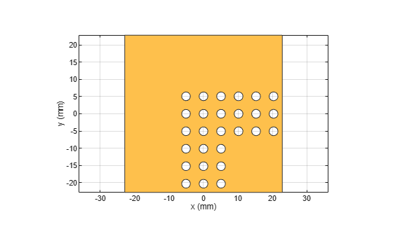
Create patch with holes of radius 25 mil
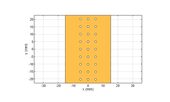
First section of the example uses a circle with radius of 25 mil as the unit etch shape on the ground. A lattice of size 3 by 9 is etched out from the ground plane. The constructed ground plane is shown below. Later section of the example shows the performance of the microstrip using circles of larger radii 50 mil and 90 mil.
gnd = boardPlane;
radius = 25*1e-3*0.0254;  % hole radius = 25mil;
posStart = [-period, -stripLength/2+period/2];
for i = 1:3
    for j =1:9
        pos = posStart+[(i-1)*period,(j-1)*period];
        circle = antenna.Circle(Radius=radius,...
             Center=pos,NumPoints=16);
        gnd = gnd - circle;
    end
end
figure
show(gnd)
axis equal;
Create PCB Stack
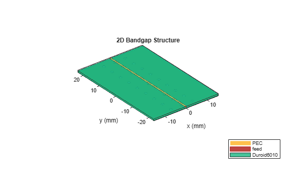
Combine the top microstrip, substrate, and etched ground plane into pcbStack object for meshing and full wave analysis. View the constructed geometry.
obj = pcbStack(Name="2D Bandgap Structure");
obj.BoardShape = boardPlane;
obj.BoardThickness = boardThick;
obj.Layers = {strip,sub,gnd};
obj.FeedLocations = [0,-boardWidth/2,1,3;0,boardWidth/2,1,3];
obj.FeedDiameter = stripWidth/2;
figure
show(obj)
axis equal;
title(obj.Name);
Manually mesh the structure using manual mesh mode to better control the output triangles and tetrahedra.
figure
mesh(obj,MaxEdgeLength=12*stripWidth,...
     MinEdgeLength=stripWidth,GrowthRate=0.85);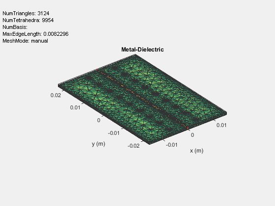
Calculate and Plot S-parameters
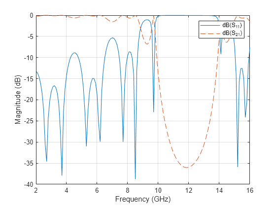
To observe the band gap effect, compute the S-parameters for the 2-port system. The band gap effect is shown in the parameter. Calculate the S-parameters from 2 GHz to 16 GHz, and plot the and for the three different circle radii. To speed up the simulation, the S-parameters have been precomputed and stored in a MAT file. The commented code shows how to calculate S-parameters. Load this MAT file and plot the S-parameters.
%% S-parameters Calculation
% freq = linspace(2e9,16e9,141);
% sparam = sparameters(obj,freq);

load('atx_bandgap_data.mat','sparam_25mil');
load('atx_bandgap_data.mat','sparam_50mil');
load('atx_bandgap_data.mat','sparam_90mil');
figure
subplot(3,1,1);
rfplot(sparam_25mil,1,1,'-');
text(4e9,-40,'Radius = 25 mil', FontSize=8, Color='m')
hold on;
rfplot(sparam_25mil,2,1,'--');
legend off;
subplot(3,1,2);
rfplot(sparam_50mil,1,1,'-');
text(4e9,-40,'Radius = 50 mil', FontSize=8, Color='m')
hold on;
rfplot(sparam_50mil,2,1,'--');
legend off;
subplot(3,1,3);
rfplot(sparam_90mil,1,1,'-');
text(4e9,-40,'Radius= 90 mil', FontSize=8, Color='m')
hold on;
rfplot(sparam_90mil,2,1,'--');
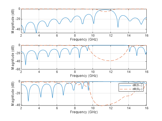
It is observed from the calculated S-parameters that there is a stop band around 11GHz, which converts the 50-ohm matched transmission line into a bandstop filter. By varying the etching shape on the groundplane, different filter structures such as low pass or high pass, etc. can be realized.
90-degree Bend Microstrip Structure
Create a compensated right-angled microstrip bend with patterned groundplane. The etched circles on the ground plane follow the right-angle bend.
Specify Board Parameters
bendboardLength = period*9;
bendboardWidth = period*9;
boardThick = 25*1e-3*0.0254; % board is 25mil thick
bendboardPlane = antenna.Rectangle(Length=bendboardLength, Width=bendboardWidth);
bendgnd = bendboardPlane;

stripLength = bendboardWidth/2;
strip_1 = antenna.Rectangle(Length=stripLength, Width=stripWidth,...
    Center=[stripLength/2,0]);
strip_2 = antenna.Rectangle(Length=stripWidth, Width=stripLength+stripWidth/2,...
    Center=[0,-stripLength/2+stripWidth/4]);

bendstrip = strip_1 + strip_2;
Create Patch with Holes of Radius 50mil
Create and view the patch with right-angle patterned holes of radius 50mil.
radius = 50*1e-3*0.0254;  % hole radius = 50mil;
posStart = [-period, -stripLength+period/2];
pos = zeros(27,2);
for i = 1:3
    for j =1:6
        pos = posStart+[(i-1)*period,(j-1)*period];
        circle = antenna.Circle(Radius=radius, Center=pos, NumPoints=15);
        bendgnd = bendgnd - circle;
    end
end
posStart = [period, -period];
for i = 1:3
    for j = 1:3
        pos = posStart+[(i)*period,(j-1)*period];
        circle = antenna.Circle(Radius=radius, Center=pos);
        bendgnd = bendgnd - circle;
    end
end
figure
show(bendgnd)
axis equal;
Use the same procedure to construct the patch with right-angle patterned holes of radius 90mil.
Create PCB Stack
Create the layer stack up by organizing the PCB layers, setting the feed locations for the ports.
bendobj = pcbStack(Name="2-D Bandgap Bend Structure");
bendobj.BoardShape = bendboardPlane;
bendobj.BoardThickness = boardThick;
bendobj.Layers = {bendstrip,sub,bendgnd};
bendobj.FeedLocations = [0,-bendboardLength/2,1,3;bendboardWidth/2,0,1,3];
bendobj.FeedDiameter = stripWidth/2;
figure
show(bendobj)
axis equal;
title(bendobj.Name);

Calculate and Plot S-parameters
To speed up the simulation, the S-parameters have been precomputed and stored in a MAT file. The commented code shows how to calculate S-parameters. Load this MAT file and plot the S-parameters. The analysis results compare favorably with the measured results reported in [1] and the PBG properties of the structure are captured effectively. It is noted here that the analysis predicts almost perfect reflection within the stop band while the measured results shown in Fig. 3 of [1] reveal the presence of a loss mechanism that improves the impedance match slightly.
%% S-parameters Calculation
% freq= linspace(2e9,16e9,141);
% sparam = sparameters(obj,freq);

load('atx_bandgap_data.mat','sparam_bend_50mil');
figure
rfplot(sparam_bend_50mil,1,1,'-');
hold on;
rfplot(sparam_bend_50mil,2,1,'--');
Conclusion
The result obtained for the three designs matches well with the result published in [1].
Reference
[1] V. Radisic, Y. Qiang, R. Coccioli, and T. Itoh, "Novel 2-D Photonic Bandgap Structure for Microstrip Lines", IEEE Microwave and Guided Wave Letters, vol. 8, No. 2, 1998;