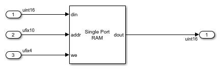
Single Port RAM System
Single-port RAM that supports sequential read and write operations

Libraries:
HDL Coder /
HDL RAMs
Alternative Configurations of Single Port RAM System Block:
Simple Dual Port RAM System | Dual Port RAM System | Simple Tri Port RAM System | True Dual Port RAM System
Description
The Single Port RAM System block models a single-port RAM that supports
sequential read and write operations. To configure this block, open the block and set
the Type of RAM parameter to Single
port. By using this block, you can:
Create parallel RAM banks by using vector data at the din, addr, and we ports.
Specify an initial value for the RAM using the Initial output of RAM parameter.
Perform asynchronous read in target hardware by selecting the Use asynchronous read feature in target hardware parameter.
Perform cycle-accurate read operation by selecting the Model RAM with one cycle of delay parameter.
Use the column-write method to write to specified bits in an addressed memory location.
Examples
This example shows how to use the column-write method to specify the writable portions of bits in an address location for Single Port RAM System block. You can then generate HDL code for the model.
Simulate Model
Load and open the column_write_sram model. The DUT subsystem contains Single Port RAM System block, the data type of the din and we ports determines the writable portion of bits in an addressed memory location.
load_system("column_write_sram");
open_system("column_write_sram/DUT");
The value at the din port is an integer with a value of 980, the value at the addr port is an integer with a value of 25, and the value at the we port is an integer with a value of 6. The binary representation of the we port value indicates that the block selects the third and second columns for writing data in the addressed memory location in the RAM. When you simulate the model, the value at the output dout port is 976. To change these values according to your requirements, see Using the Column-Write Method to Selectively Write to Columns.
sim('column_write_sram.slx');
open_system("column_write_sram");

Generate HDL code
Use HDL Coder™ to generate the HDL code for the model. To generate HDL code for DUT subsystem, run this makehdl command:
makehdl("column_write_sram/DUT");
### Working on the model <a href="matlab:open_system('column_write_sram')">column_write_sram</a>
### Generating HDL for <a href="matlab:open_system('column_write_sram/DUT')">column_write_sram/DUT</a>
### Using the config set for model <a href="matlab:configset.showParameterGroup('column_write_sram', { 'HDL Code Generation' } )">column_write_sram</a> for HDL code generation parameters.
### Running HDL checks on the model 'column_write_sram'.
### Begin compilation of the model 'column_write_sram'...
### Working on the model 'column_write_sram'...
### Working on... <a href="matlab:configset.internal.open('column_write_sram', 'GenerateModel')">GenerateModel</a>
### Begin model generation 'gm_column_write_sram'...
### Copying DUT to the generated model....
### Model generation complete.
### Generated model saved at <a href="matlab:open_system('hdlsrc/column_write_sram/gm_column_write_sram.slx')">hdlsrc/column_write_sram/gm_column_write_sram.slx</a>
### Begin VHDL Code Generation for 'column_write_sram'.
### Working on column_write_sram/DUT/SinglePortRAM_generic as hdlsrc/column_write_sram/SinglePortRAM_generic.vhd.
### Working on column_write_sram/DUT as hdlsrc/column_write_sram/DUT.vhd.
### Code Generation for 'column_write_sram' completed.
### Generating HTML files for code generation report at <a href="matlab:hdlcoder.report.openReportV2Dialog('/tmp/Bdoc26a_3233028_1586746/tpae415596/hdlcoder-ex10710190/hdlsrc/column_write_sram', '/tmp/Bdoc26a_3233028_1586746/tpae415596/hdlcoder-ex10710190/hdlsrc/column_write_sram/html/index.html')">index.html</a>
### Creating HDL Code Generation Check Report file:///tmp/Bdoc26a_3233028_1586746/tpae415596/hdlcoder-ex10710190/hdlsrc/column_write_sram/DUT_report.html
### HDL check for 'column_write_sram' complete with 0 errors, 1 warnings, and 0 messages.
### HDL code generation complete.
Limitations
When you build the FPGA bitstream for the RAM, the global reset logic does not reset the RAM contents. To reset the RAM, implement the reset logic.
The RAM address can be either
fixed-point (fi)orinteger, must be unsigned, and must be between2and31bits long.