Modeling Efficient Multiplication and Division Operations for FPGA Targeting
These guidelines illustrate the recommended settings when using Divide and Product blocks in your model for improved area and timing on the target FPGA. Each guideline has a severity level that indicates the level of compliance requirements. To learn more, see HDL Modeling Guidelines Severity Levels.
Designing Multipliers and Adders for Efficient Mapping to DSP Blocks on FPGA
Guideline ID
2.7.1
Severity
Strongly Recommended
Description
Digital signal processing (DSP) algorithms use several multipliers and accumulators. FPGA devices provided by vendors such as Xilinx® and Intel® contain dedicated DSP slices. These small size, high speed, DSP slices contain several multipliers and accumulators that make FPGA devices best suited for DSP applications.
The architecture of DSP slices varies widely across the different FPGA vendors and across different families of devices provided by the same vendor. To map your Simulink® model containing adders, multipliers, and delays to DSP slices, adapt your model to the DSP slice architecture by taking into consideration:
Arrangement of flipflops, adders, and multipliers in the DSP slice.
Rounding and saturation settings.
Bit widths of the adders and multipliers. For efficient mapping, use bit widths in your model that are less than or equal to the bit widths of the DSP unit.
When the bit widths in your model become larger than the bit widths of the DSP, your design does not fit onto one DSP. In this case, multiple DSPs or additional logic is required.
You can map these blocks in your model to DSP blocks on an FPGA:
Add and Sum
Delay
Product
Multiply-Add
Multiply-Accumulate
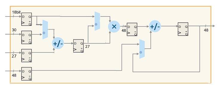
Architecture of DSP48E1 Slice
This figure illustrates the Xilinx DSP architecture. Xilinx 7 series FPGAs have dedicated DSP slices that use this architecture. The DSP architecture consists of input registers, pre-adder, 25x18 multiplier, intermediate registers, post-adder, and an output register.

For more information, see DSP48E1 Slice Overview in the Xilinx documentation.
Architecture of DSP48E2 Slice
This figure illustrates the Xilinx DSP architecture. Xilinx UltraScale® series FPGAs have dedicated DSP slices that use this architecture. The DSP architecture consists of input registers, pre-adder, 27x18 multiplier, intermediate registers, post-adder, and an output register.
For more information, see UltraScale Architecture DSP Slice Overview in the Xilinx documentation.
Architecture of Stratix® V devices
This figure illustrates the Intel DSP architecture. This DSP architecture for Stratix® V devices is a variable precision DSP architecture. The DSP blocks can have bit widths of 9, 18, 27, and 36 bits, and 18x25 complex multiplication for FFTs.

For more information, see DSP Block Architecture of Stratix V devices.
Algorithm Design
To learn how you can design your algorithm to map to this DSP unit, open the model hdlcoder_multiplier_adder_dsp.slx.
open_system('hdlcoder_multiplier_adder_dsp');
set_param('hdlcoder_multiplier_adder_dsp', 'SimulationCommand', 'Update');
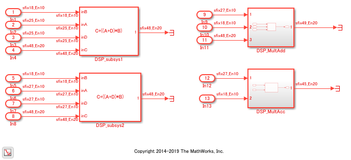
The model consists of two subsystems DSP_subsys1 and DSP_subsys2 which implement the operation C+((A+D)*B. You can also implement this operation by using Multiply-Add or Multiply-Accumulate blocks, as illustrated by subsystems DSP_MultAdd and DSP_MultAcc.
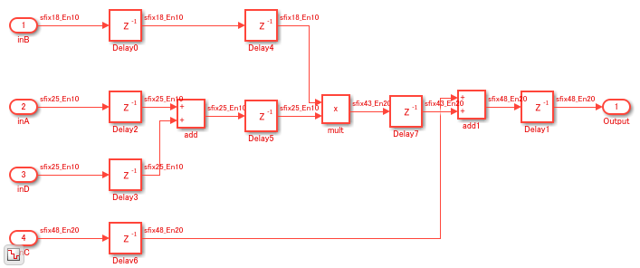
To see the implementation of the operation C+((A+D)*B, open the model DSP_subsys1.
open_system('hdlcoder_multiplier_adder_dsp/DSP_subsys1');
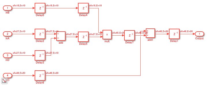
To see the implementation of the operation C+((A+D)*B, open the model DSP_subsys2.
open_system('hdlcoder_multiplier_adder_dsp/DSP_subsys2');
Implementation on Xilinx 7 series FPGA
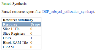
The DSP_subsys1 implements the operation C+((A+D)*B by using bit widths that match the DSP on a Xilinx 7 series FPGA. If you open the HDL Workflow Advisor and deploy this subsystem onto a Xilinx Virtex® 7 FPGA, the entire design fits exactly onto a single DSP slice.
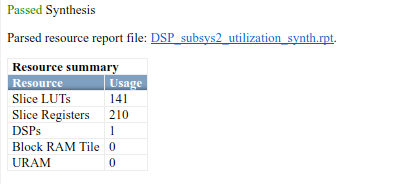
The DSP_subsys2 implements the same operation by using bit widths that are larger than the DSP on a Xilinx FPGA. If you deploy this subsystem onto a Xilinx Virtex 7 FPGA, you will see that the entire design does not fit into a single DSP slice and instead uses additional slice logic.
Implementation on Xilinx UltraScale FPGA
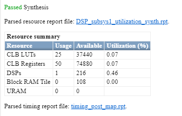
The DSP_subsys1 implements the operation C+((A+D)*B by using bit widths that are less than those of the DSP on a Xilinx UltraScale FPGA. If you open the HDL Workflow Advisor and deploy this subsystem onto a Xilinx Artix UltraScale® FPGA, the entire design does not fits onto a single DSP slice and instead uses additional logic.
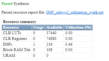
The DSP_subsys2 implements the same operation by using bit widths that match the DSP on a Xilinx UltraScale FPGA. If you deploy this subsystem onto a Xilinx Artix UltraScale® FPGA, you will see that the entire design fits onto a single DSP slice.
Set ConstMultiplierOptimization HDL Block Property to auto for Gain Block
Guideline ID
2.7.2
Severity
Strongly Recommended
Description
When you use a Gain block in your design, to achieve the most
area-efficient implementation, set the ConstMultiplierOptimization HDL block property to
auto. The code generator chooses between
CSD and FCSD
implementations that yields the smallest circuit size and generates HDL code
without using the multiplication (*) operator.
You can use this setting to avoid targeting DSP resources and reduce the number of logic circuits on Intel® Quartus® Prime when synthesizing your design on the target FPGA. For example, this table shows the generated HDL code for the Gain block depending on the HDL block property settings for the ConstMultiplierOptimization block.

ConstMultiplierOptimization Settings and Impact on Generated HDL Code
ConstMultiplierOptimization
Setting | Operations | Generated HDL Code |
|---|---|---|
CSD | Casts input data in parallel and adds or subtract the results.
| This code shows the generated VHDL code. -- CSD Encoding(231): 1001'01001'; Cost (Adders) = 3 DOUT_mul_temp <= ((resize(DIN & '0' & '0' & '0' & '0' & '0' & '0' & '0' & '0', 21) - resize(DIN & '0' & '0' & '0' & '0' & '0', 21)) + resize(DIN & '0' & '0' & '0', 21)) - resize(DIN, 21); DOUT <= DOUT_mul_temp(19 DOWNTO 0); This code shows the generated Verilog code. // CSD Encoding (231) : 1001'01001'; Cost (Adders) = 3
assign Gain_1 = {DIN[11], {DIN, 8'b00000000}};
assign Gain_2 = {{4{DIN[11]}}, {DIN, 5'b00000}};
assign Gain_3 = {{6{DIN[11]}}, {DIN, 3'b000}};
assign Gain_4 = {{9{DIN[11]}}, DIN};
assign DOUT_mul_temp = ((Gain_1 - Gain_2) + Gain_3) - Gain_4;
assign DOUT = DOUT_mul_temp[19:0];
|
FCSD | Adds the input data and its cast data in each cascading.
| This code shows the generated VHDL code. -- FCSD for 231 = 33 X 7; Total Cost = 2 -- CSD Encoding (33) : 0100001; Cost (Adders) = 1 Gain_factor <= resize(DIN & '0' & '0' & '0' & '0' & '0', 21) + resize(DIN, 21); -- CSD Encoding (7) : 1001'; Cost (Adders) = 1 DOUT_mul_temp <= resize(Gain_factor & '0' & '0' & '0', 21) - Gain_factor; DOUT <= DOUT_mul_temp(19 DOWNTO 0); This code shows the generated Verilog code. // FCSD for 231 = 33 X 7; Total Cost = 2
// CSD Encoding (33) : 0100001; Cost (Adders) = 1
assign Gain_3 = {{4{DIN[11]}}, {DIN, 5'b00000}};
assign Gain_4 = {{9{DIN[11]}}, DIN};
assign Gain_factor = Gain_3 + Gain_4;
// CSD Encoding (7) : 1001'; Cost (Adders) = 1
assign Gain_1 = {Gain_factor, 3'b000};
assign Gain_2 = Gain_1[20:0];
assign DOUT_mul_temp = Gain_2 - Gain_factor;
assign DOUT = DOUT_mul_temp[19:0];
|
auto | Selects CSD or FCSD implementation that uses fewer adders. | Generated HDL code is same as CSD or FCSD implementation. |
none | Uses multiplication operator (*). | This code shows the generated VHDL code. DOUT_mul_temp <= to_signed(2#011100111#, 9) * DIN; DOUT <= DOUT_mul_temp(19 DOWNTO 0); This code shows the generated Verilog code. assign DOUT_mul_temp = 231 * DIN; assign DOUT = DOUT_mul_temp[19:0]; |
Use ShiftAdd Architecture of Divide Block for Fixed-Point Types
Guideline ID
2.7.3
Severity
Recommended
Description
When you use fixed-point data types as inputs to the Divide block, specify the HDL
Architecture of the block as ShiftAdd. In this architecture,
the block computes the result by using multiple shift and add operations. The
operations are pipelined to achieve higher clock frequencies on the target FPGA
device.
When you use floating-point data types as inputs to the Divide block, select Use Floating Point configuration parameter.
Use Gain Block for Fixed-Point Constant Operations
Guideline ID
2.7.4
Severity
Strongly Recommended
Description
When you use the Constant block configured with fixed-point data types as an input to the Product, Divide, or Trigonometric operation blocks, you can replace those operators with a Gain or Constant block to reduce the circuit area of your design. You can use these design considerations for blocks with constant input:
When one input of the Product block is a Constant block, replace the Product block with a Gain block and set the constant value as the Gain value of the Gain block.
When the divisor input of the Divide block is a Constant block, replace the Divide block with a Gain block and set the reciprocal of the constant value to the Gain value of the Gain block.
When the input to the Trigonometric Function block, such as
sin,cos, oratan2is a Constant block, replace the block with a Constant block and set the calculated values to the Constant block. For example, if the input to the Sin block isπ/3, replace the Sin block with a Constant block and set the constant value tosin(pi/3).
The circuit area required for variable and constant operations are different. Using the constant operations can reduce the circuit area of your design.