Get Started with RF PCB Toolbox
RF PCB Toolbox™ provides functions and apps for designing, analyzing, and visualizing high-speed and RF multilayer printed circuit boards (PCBs). You can model coupling, dispersion, losses, and DC performance using electromagnetic analysis techniques such as the frequency-domain Method of Moments and the Finite Element Method. Fast frequency sweeps enable efficient electromagnetic analysis across broadband frequency ranges.
Designers of RF boards, MMICs, and SiPs can use a library of layout primitives and parameterized components, such as traces, filters, couplers, and vias, to predict PCB performance and generate Gerber files. Integration with RF Blockset™ allows wireless system architects to perform simulation and performance verification of end-to-end communications and radar systems.
The toolbox works with PCB and package database formats, including ODB++, Cadence® Allegro®, and others, enabling signal integrity engineers to analyze high-speed PCB layouts.
Tutorials
- Rat-Race Coupler - Visualize and Analyze
Create and view an object from the components catalog.
- Use Metal Catalog to Design Coplanar Waveguide
Use the materials catalog to enable the selection of conductor metals and substrate dielectric materials for PCB objects.
- Create Default Curved Bend Shape
Create custom PCB geometry objects.
- Calculate S-parameters for Wilkinson Power Splitter
Analyze PCB objects.
- Import and View Top Layer Gerber File
Import PCB files.
- Design Chebyshev Hairpin Filter at 1.8 GHz
Design a PCB object around a specified frequency.
RF PCB Concepts
- Scattering Parameters or S-Parameters
Basics of S-parameters, how to analyze PCB components using S-parameters. - Behavioral Models
Accelerate circuit level analysis, behavioral s-parameter calculations, optimize layout and performance. - Characteristic Impedance of Transmission Lines
Characteristic impedance of transmission lines; even and odd mode impedances of coupled transmission lines. - PCB Feeds
Basics of PCB signal feeds, including feed type definitions and applications of each feed type. - Overview of Solvers
RF PCB Toolbox provides four electromagnetic solvers to support different applications. - Method of Moments Solver for Metal and Dielectric Structures
Method of Moments computation technique for metal and dielectrics in a PCB. - 2-D Field Solver
The 2-D field solver in RF PCB Toolbox™ allows you to model and analyze the cross-sections of multi-conductor transmission lines in a multi-layered dielectric above a ground plane like a microstrip line. - Eigenmode-Based Solver for PCB Vias
Wave generation and propagation in vias, circuit model, equations. - FEM-based Solver for RF Structures
This topic explains the use of a Finite-Element-Method-based solver to complex RF structures.
Fundamental RF PCB Analysis
Solvers
Featured Examples
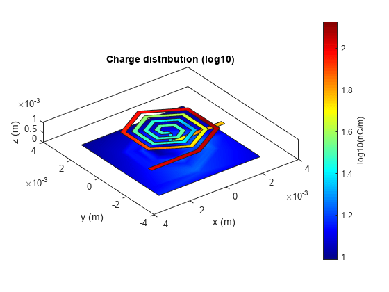
Introduction to Passive Planar Spiral Inductors
Design and analyze a passive planar spiral inductor.

Introduction to Equal and Unequal Split Wilkinson Power Splitter
Design, analyze, and compare an equal and unequal Wilkinson splitter.

Introduction to 4-Port Couplers
Design and analyze 4-Port couplers.