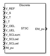
SM ST3C
Discrete- or continuous-time synchronous machine ST3C or ST3A static excitation system with an automatic voltage regulator
Libraries:
Simscape /
Electrical /
Control /
SM Control
Description
The SM ST3C block implements a synchronous machine (SM) ST3C static excitation system model in conformance with IEEE Std 421.5-2016 [1]. You can also use the SM ST3C block to implement an ST3A model from previous versions of IEEE Std 421.5 [2-3]. For more information about implementing an ST3A model, see ST3A Model.
Use this block to model the control and regulation of the field voltage of a synchronous machine.
You can switch between continuous and discrete implementations of the block by using the
Sample time (-1 for inherited) parameter. To configure the
integrator for continuous time, set the Sample time (-1 for
inherited) property to 0. To configure the integrator
for discrete time, set the Sample time (-1 for inherited) property
to a positive, nonzero value, or to -1 to inherit the sample time
from an upstream block.
The SM ST3C block comprises four major components:
The Current Compensator modifies the measured terminal voltage as a function of the terminal current.
The Voltage Measurement Transducer simulates the dynamics of a terminal voltage transducer using a low-pass filter.
The Excitation Control Elements component compares the voltage transducer output with a terminal voltage reference to produce a voltage error. This voltage error is then passed through a voltage regulator to produce the field voltage.
The Power Source models the power source for the controlled rectifier when it is independent from the terminal voltage.
This diagram shows the overall structure of the ST3C excitation system model:
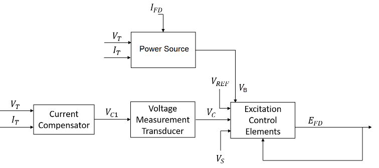
In the diagram:
VT and IT are the measured terminal voltage and current of the synchronous machine.
VC1 is the current-compensated terminal voltage.
VC is the filtered, current-compensated terminal voltage.
VREF is the reference terminal voltage.
VS is the power system stabilizer voltage.
VB is the exciter field voltage.
EFD and IFD are the field voltage and current, respectively.
The following sections describe each of the major parts of the block in detail.
Current Compensator and Voltage Measurement Transducer
The current compensator is modeled as:
where:
RC is the load compensation resistance.
XC is the load compensation reactance.
The voltage measurement transducer is implemented as a Low-Pass Filter block with the time constant TR. Refer to the documentation for the Low-Pass Filter block for the discrete and continuous implementations.
Excitation Control Elements
This diagram illustrates the overall structure of the excitation control elements:
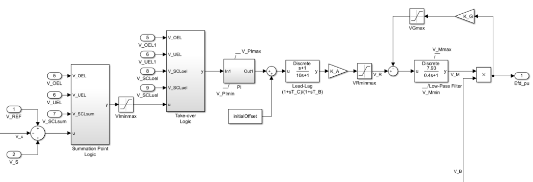
In the diagram:
The Summation Point Logic subsystem models the summation point input location for the overexcitation limiter (OEL), underexcitation limiter (UEL), stator current limiter (SCL), and the power switch selector (V_S) voltages. For more information about using limiters with this block, see Field Current Limiters.
The Take-over Logic subsystem models the take-over point input location for the OEL, UEL, and SCL voltages. For more information about using limiters with this block, see Field Current Limiters.
The PI subsystem models a PI controller that functions as a control structure for the automatic voltage regulator and allows the representation of an equipment retrofit with a modern digital controller. The minimum and maximum anti-windup saturation limits for the block are VPImin and VPImax, respectively.
The Lead-Lag block models additional dynamics associated with the voltage regulator and represents the system stabilizer. Here, TC is the lead time constant and TB is the lag time constant. Refer to the documentation for this block for the exact discrete and continuous implementations.
An inner field voltage control loop is utilized to linearize the exciter control characteristic and it is composed of the gains KM and KG and the time constant TM. The minimum and maximum anti-windup saturation limits for the block are VMmin and VMmax, respectively.
Field Current Limiters
You can use various field current limiters to modify the output of the voltage regulator under unsafe operating conditions:
Use an overexcitation limiter to prevent overheating of the field winding due to excessive field current demand.
Use an underexcitation limiter to boost field excitation when it is too low, which risks desynchronization.
Use a stator current limiter to prevent overheating of the stator windings due to excessive current.
Attach the output of any of these limiters at one of these points:
The summation point as part of the automatic voltage regulator (AVR) feedback loop
The take-over point to override the usual behavior of the AVR
If you are using the stator current limiter at the summation point, use the single input VSCLsum. If you are using the stator current limiter at the take-over point, use both the overexcitation input, VSCLoel, and the underexcitation input, VSCLuel.
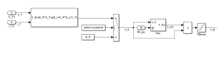
Power Source
It is possible to adopt a different representation of the power source for the controlled
rectifier by selecting the relevant option in the Power source
selector parameter. The power source for the controlled rectifier can
be either derived from the terminal voltage (Position A: power source
derived from generator terminal voltage) or it can be independent
of the terminal voltage (Position B: power source independent of
generator terminal conditions).
This diagram shows a model of the exciter power source utilizing a phasor combination of the terminal voltage, VT, and terminal current, IT:
ST3A Model
You can represent existing ST3A static excitation systems using the ST3C model. The ST3C model added the PI controller for the voltage regulator. The model also introduced additional options for the OEL, UEL, and SCL input locations. To implement an ST3A model using the SM ST3C block, set the parameters to the values shown in this table.
| Block Parameter | Parameter Value |
|---|---|
| Voltage regulator proportional gain, K_PR (pu) | 1 |
| Voltage regulator integral gain, K_IR (pu/s) | 0 |
| Maximum voltage regulator output, V_PImax (pu) | 99 |
| Minimum voltage regulator output, V_PImin (pu) | -99 |
| Alternate OEL input locations (V_OEL) | Unused |
| Alternate UEL input locations (V_UEL) | Unused or
Take-over |
| Alternate SCL input locations (V_SCL) | Unused |
Note
The ST3C model moved the block that represents the dynamic response of the
controlled rectifier bridge to the output. This can cause differences in the
dynamic response of the ST3C and ST3A models. To obtain identical results, set
the Feedback gain of field current regulator, K_G (pu)
parameter to 0. Setting
KG equal to zero is not a
requirement of the ST3A model, but you may see some discrepancies with the ST3C
model for nonzero values.
Ports
Input
Output
Parameters
References
[1] “IEEE Recommended Practice for Excitation System Models for Power System Stability Studies.” IEEE Std 421.5-2016 (Revision of IEEE Std 421.5-2005), August 2016, 1–207. https://doi.org/10.1109/IEEESTD.2016.7553421.
[2] “IEEE Recommended Practice for Excitation System Models for Power System Stability Studies.” IEEE Std 421.5-2005 (Revision of IEEE Std 421.5-1992), April 2006, 1–93. https://doi.org/10.1109/IEEESTD.2006.99499.
[3] “IEEE Recommended Practice for Excitation System Models for Power System Stability Studies.” IEEE Std 421.5-1992, August 1992, 1–56. https://doi.org/10.1109/IEEESTD.1992.106975.
Extended Capabilities
Version History
Introduced in R2020a