Differential Pair Amplifier
This example shows a differential pair amplifier circuit. The circuit can be used to explore the properties of a differential pair amplifier. The model can be tested using differential and common-mode inputs. The balanced output has zero gain in common-mode provided that the two transistors have identical properties.
Transistor NPN 3 acts as a constant current source that helps stabilize differential-mode gain. The combination of R1, R3 and D1 sets the base voltage to about 1V above the negative power rail. The base-emitter saturation voltage is 0.4V, and hence the voltage across R2 is 0.6V giving an emitter current of 0.6/220=2.7mA. D1 provides temperature compensation, the forward voltage variation with temperature being similar to that of the base-emitter junction. Transistor component values are typical for a BC107, and the diode component values are typical for an IN4148.
This model can be used to obtain the frequency response of the system. The Solver Configuration block option "Start simulation from steady state" is enabled to ensure that the model is linearized about its nominal operating point. MATLAB® command linmod can be used to linearize the model. If you have Simulink® Control Design™, open the model DifferentialPairAmplifier. On the Apps tab, under Control Systems, click Model Linearizer. In the Model Linearizer, on the Linear Analysis tab, in the Linearize section, click Bode. The linearization points are defined by right-clicking on a Simulink line, and selecting Linearization Points. If you look at the Sensor block, you will see the linearization output symbol at the output of the PS-Simulink block. Similarly under the Source block you will see a linearization input point symbol on the output of the Sine Wave block.
Model

Simulation Results from Simscape Logging
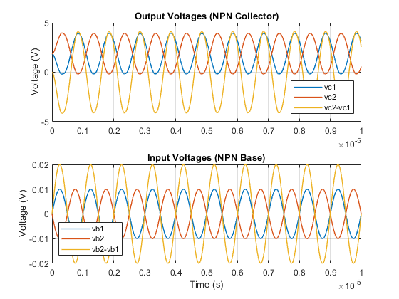
The plot below shows the output and input of the differential pair amplifier model. The difference in the base voltages (vb2-vb1) is amplified by more than a factor of 40. The output is measured as the difference between the two collector outputs (vc2-vc1).

Frequency Response

See Also
NPN Bipolar Transistor | Negative Supply Rail | Positive Supply Rail