C2000 DC-DC Buck Converter Using MCU
This example shows how to develop a DC-DC buck converter power regulator application. Typical challenges with power conversion simulation and deployment include:
Modeling the analog circuit behavior of the buck converter circuit
Modeling the timing behavior of PWM output and ADC sampling on an MCU
Capturing signals in high CPU load controllers
The amount of time required for controller validation, which is typically performed on hardware
These challenges are addressed in this example using C2000™ Microcontroller Blockset and Simscape™. Digital control type used in this example is voltage mode controller (VMC), verified on the TI Delfino F28379D LaunchPad and TI BOOSTXL-BUCKCONV kit.
Required Hardware
Hardware Connections
Connect the Digital Power Buck Converter BoosterPack (BOOSTXL-BUCKCONV) to the Texas Instruments Delfino F28379D LaunchPad as detailed in the following table.

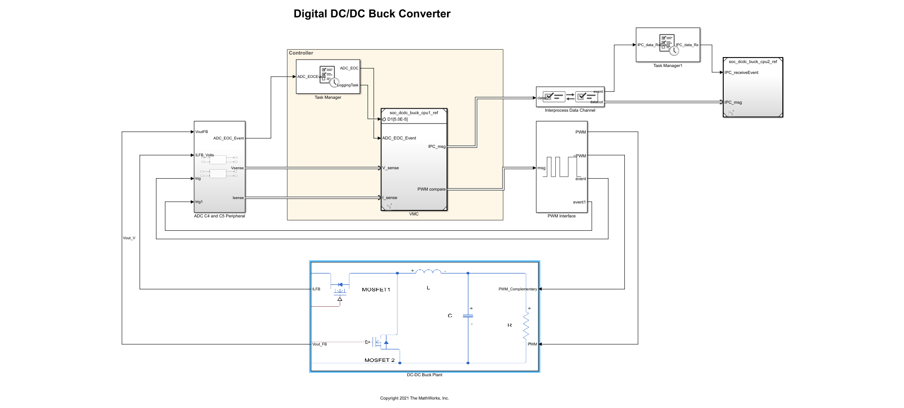
This model shows the complete converter system, and the sections in this example will examine the individual challenges. Open the soc_dcdc_buck model.

Model of DC-DC Buck Converter Kit
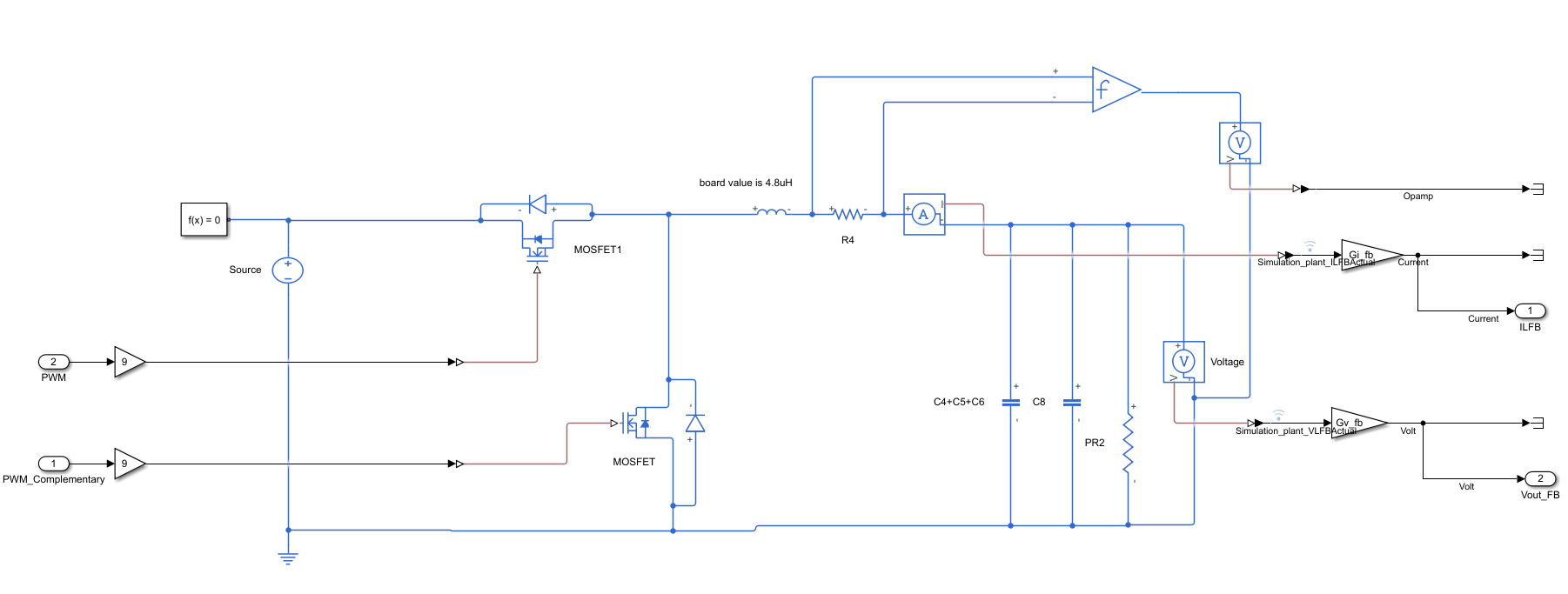
DC-DC Buck Plant subsystem is a Simscape reference model of the DC-DC buck converter analog circuitry.

The Simscape™ blocks in the model are selected and configured based on the original equipment manufacturer (OEM) specifications provided in the data sheet. To achieve computational efficiency in simulation without affect on behavior, the model includes these simplification relative to OEM specifications:
Voltage and current sensing circuits are simplified to gain blocks.
MOSFETS are simplified to ideal MOSFETS.
Gate driver is not modeled and its propagation delays are not considered.
Inductor is simplified to linear inductor.
All parts are modeled with nominal values, and tolerances are not considered.
DC supply is assumed to be constant.
If needed, the open loop response of the Simscape model can be compared and verified against the physical hardware using a digital oscilloscope with results captured using the Data Acquisition Toolbox.
Voltage Mode Control on MCU
On the MCU, the output of the plant sampled by the ADC Interface generating an event on each end of conversion. The Task Manager executes an event-driven task called ADC upon reception of each ADC end-of-conversion event. The ADC Interrupt task contains the feedback control algorithm that executes asynchronously in response to each ADC conversion event. The control algorithm receives feedback through ADC Read and generates duty cycle values for PWM Write block. The PWM Interface block simulates PWM behavior including triggering an event to start the next ADC conversion. PWM frequency is set to 200 kHz. The discrete proportional integral (PI) controller minimizes the error between the reference voltage and the output voltage. The duty cycle of the PI controller is limited to 40% of the PWM time period.
The system starts with an initial voltage reference of 1 volt and allowed to reach steady state. This enables a fair control between the physical hardware and simulation to compare with a known state. The desired voltage step of 2 volts is then triggered at 50 ms to examine the step response of the closed loop controller. Click Play to simulate the model. Open the Simulation Data Inspector and view signals.
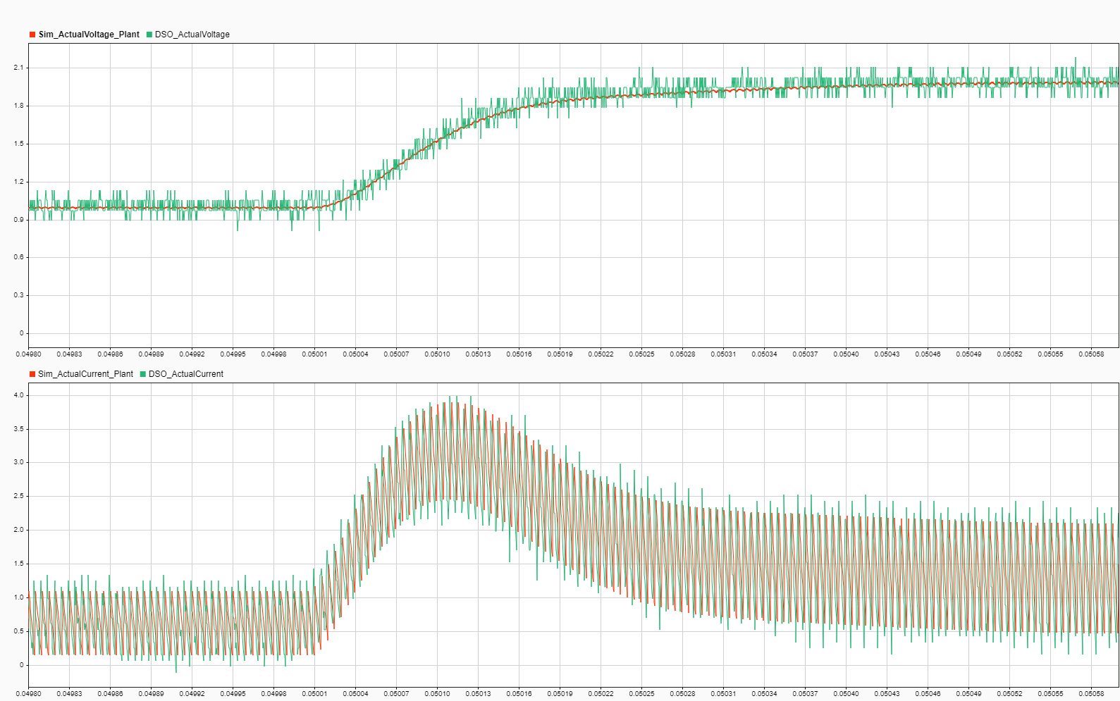
To verify simulation results against hardware, deploy the model to the Texas Instruments Delfino F28379D LaunchPad. On the System on Chip tab, click Configure, Build, & Deploy to open the SoC Builder tool. This figure shows the comparison of the controller response between the simulation and deployed model on the physical hardware. This signal on the hardware is captured using a digital oscilloscope. The high frequency operation of controller prevents the direct use of external mode on the same CPU. For this reason a digital oscilloscope is used to take these measurements.

As expected, the voltage mode controller correctly tracks the desired the voltage output. Additionally the measurements from the deployed model match the simulation with greater than 95% accuracy for this type of system. The minor differences seen between the simulation and the deployed measurements can be attributed to the simplifications made in the Simscape model.
Taking Advantage of Multicore to Log Data in CPU2
CPU2 is configured to run external mode SoC Builder tool, to log and transmit the high frequency signals produced by control loop on CPU1. An Interprocess Data Channel block connects CPU1 and CPU2, providing a low latency data transfer between the CPUs.
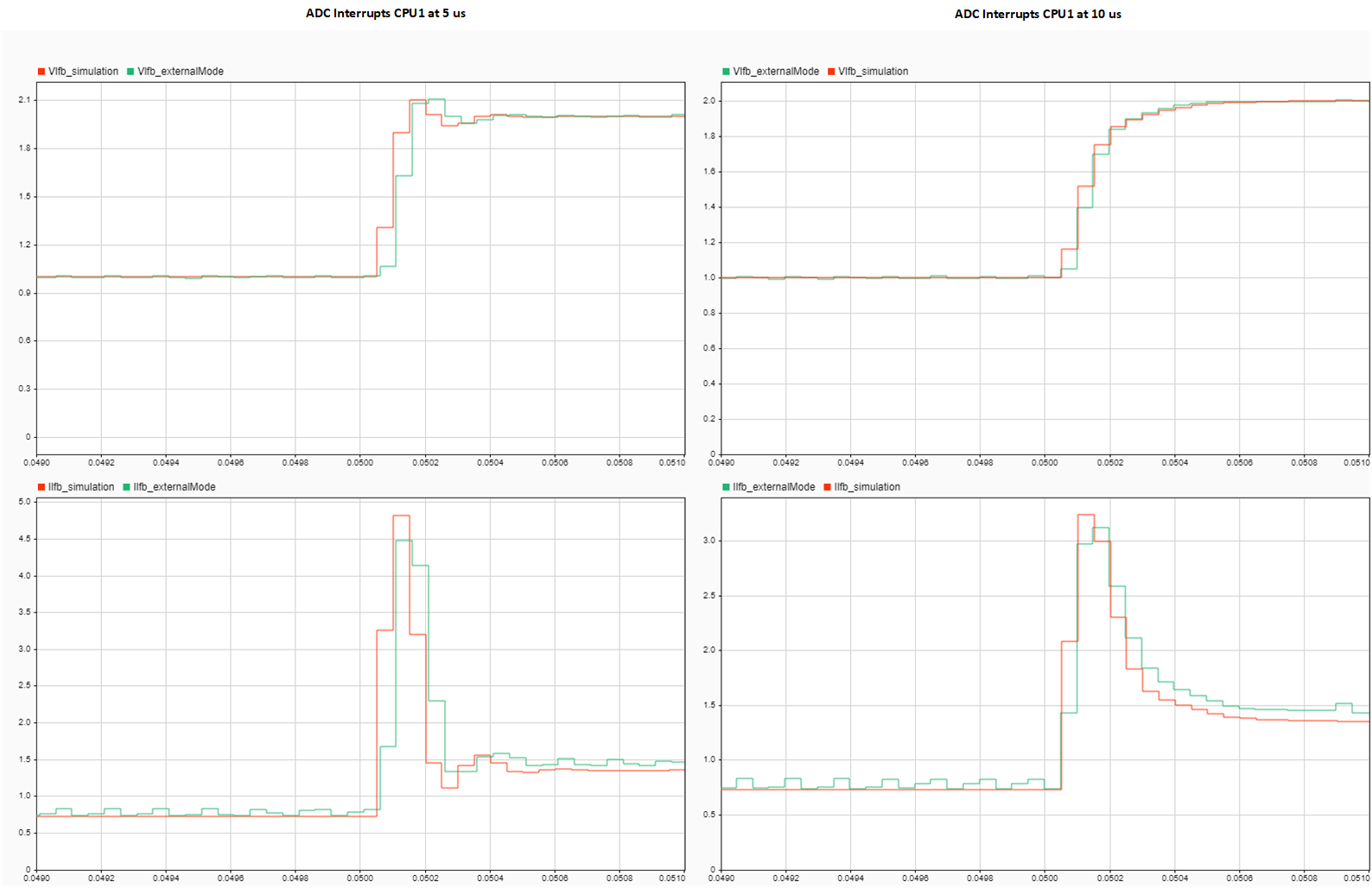
Use the SoC Builder tool to deploy the model to the TI Delfino F28379D LaunchPad. A host-target communication connection, set up by the SoC Builder tool, logs the signal data from the executable running on CPU2 of the hardware board and sends the data to the Simulation Data Inspector in Simulink. Using CPU2 to own and manage the host-target communication and data logging, data can be captured from the resource intensive, high-priority task on CPU1 without interfering with its behavior and enabling that task to consume most of the CPU resources, and with maintaining the quality of data logging to Simulink. This figure shows the logged data signal from task 1 on CPU1, captured on task 2 on CPU2, of the model deployed to a TI Delfino F28379D LaunchPad.

ADC start of conversion trigger can be configured to generate at 1st PWM or 2nd PWM event. These settings are available in simulation and codegen. Observe simulation and codegen results match with greater than 95% accuracy.
Any resource intensive C2000 Blockset model could use this setup to log data from hardware when the model is deployed to a TI Delfino F28379D LaunchPad.
Further Exploration
Extend for high frequency switching applications involving Gallium Nitride (GaN) or Silicon Carbide (SiC)
Variable PWM frequency and fixed duty cycle
Variable phase offset
Different PWM output schemes by using the PWM output control options
Different PWM event generation techniques