Patch Antenna with Dielectric Substrate
This example shows how to create linearly-polarized rectangular patch antennas with custom dielectric substrate and compares their performance with results in [1]. The first antenna has a low-epsilon thin dielectric substrate while the second antenna has a thick high-epsilon dielectric substrate.
Create Patch Antenna with Low-Epsilon Thin Substrate
Create a rectangular patch antenna with a length of 40 mm and a width of 30 mm on a 80 mm-by-60 mm ground plane. The lossless substrate has a dielectric constant of 2.33 and thickness of 1.57 mm. The feed is offset by 5.5 mm from the origin along the x-axis.
p1 = patchMicrostrip;
p1.Length = 40e-3;
p1.Width = 30e-3;
p1.Height = 1.57e-3;
p1.GroundPlaneLength = 80e-3;
p1.GroundPlaneWidth = 60e-3;
p1.FeedOffset = [5.5e-3 0];
Antenna Toolbox™ has a list of substrates supported as part of its dielectric catalog. To open the catalog use the following command.
openDielectricCatalog
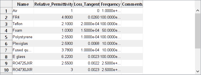
The substrate specified for this patch is not part of the dielectric catalog. You can add it to the catalog if desired, so that the material can be used next time without specifying its electrical properties. You can also specify the substrate property directly as well as shown below.
p1.Substrate = dielectric(Name="material1",EpsilonR=2.33);As indicated in the reference [1], the feed is modeled as a square column of side 1mm. This feed model is available in the pcbStack. Convert the patch model to the stack representation and model the feed.
pb1 = pcbStack(p1);
pb1.FeedDiameter = sqrt(2)*1e-3;
pb1.FeedViaModel = "square"
pb1 =
pcbStack with properties:
Name: 'Probe-fed rectangular microstrip patch'
Revision: 'v1.0'
BoardShape: [1×1 antenna.Rectangle]
BoardThickness: 0.0016
Layers: {[1×1 antenna.Rectangle] [1×1 dielectric] [1×1 antenna.Rectangle]}
FeedLocations: [0.0055 0 1 3]
FeedDiameter: 0.0014
ViaLocations: []
ViaDiameter: []
FeedViaModel: 'square'
FeedVoltage: 1
FeedPhase: 0
Conductor: [1×1 metal]
Tilt: 0
TiltAxis: [1 0 0]
Load: [1×1 lumpedElement]
SolverType: 'MoM'
figure
show(pb1)
title("Patch Antenna with Thin Substrate")
Analyze Thin Patch Antenna Performance
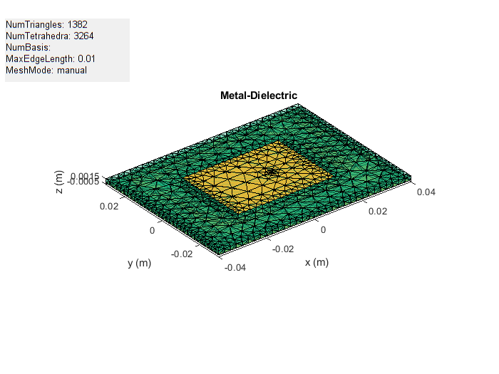
Mesh the structure by specifying the maximum and the minimum edge lengths. Below is the mesh used to model the antenna. The triangles are used to discretize the metal regions of the patch, and tetrahedra are used to discretize the volume of the dielectric substrate in the patch. These are indicated by the colors yellow and green respectively. The total number of unknowns is the sum of the unknowns for the metal plus the unknowns used for the dielectric. As a result, the time to calculate the solution increases significantly as compared to pure metal antennas.
figure
mesh(pb1,MaxEdgeLength=0.01,MinEdgeLength=0.003)
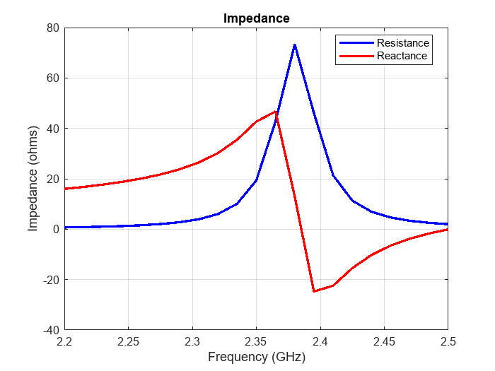
The impedance of the antenna shows a resonance at 2.37 GHz. This value is very close to the results published in the paper.
figure
impedance(pb1,linspace(2.2e9,2.5e9,21))
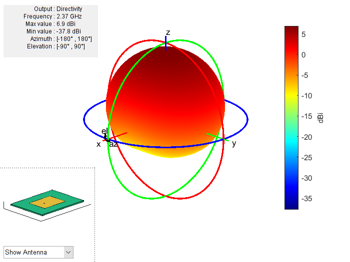
The antenna pattern at resonance also shows uniform illumination above the ground plane with minimum leakage below it.
figure
pattern(pb1,2.37e9)
Modeling Thin vs. Thick Dielectric Substrates
Thickness of a dielectric substrate is measured with respect to the wavelength. In the case above, the wavelength in free-space is about 126 mm. The wavelength in dielectric is approximated by dividing the above number by the square root of the dielectric constant. This value is about 85 mm. So the substrate thickness is about 1/50th of the wavelength in dielectric. This is a thin substrate.
The next case considers a patch antenna on a substrate whose thickness is 1/10th of the wavelength in dielectric. This is a thick substrate. A method of moments solver requires at least 10 elements per wavelength to give an accurate solution. So if the dielectric thickness becomes greater than this, the solution accuracy is affected. In the Antenna Toolbox if the substrate thickness is greater than 1/10th of the wavelength in dielectric, manual meshing is recommended for solving the antenna structure. As the 10 element per wavelength criteria is not satisfied, a certain amount of error in the solution is expected.
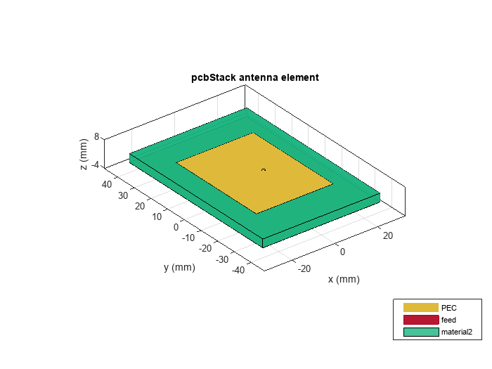
Create Patch Antenna with High-Epsilon Thick Substrate
Create a rectangular patch antenna with a length of 36 mm and a width of 48 mm on a 55 mm-by-80 mm ground plane. The lossless substrate has a dielectric constant of 9.29 and thickness of 3.82mm. The feed is offset by 4 mm from the origin along the x-axis. Similar to the previous case, convert the model to the stack representation and change the feed model as noted in [1].
p2 = patchMicrostrip;
p2.Length = 36e-3;
p2.Width = 48e-3;
p2.Height = 3.82e-3;
p2.GroundPlaneLength = 55e-3;
p2.GroundPlaneWidth = 80e-3;
p2.FeedOffset = [4.0e-3 0];
p2.Substrate = dielectric(Name="material2",EpsilonR=9.29);
pb2 = pcbStack(p2);
pb2.Layers{1}.NumPoints = 40;
pb2.Layers{3}.NumPoints = 40;
pb2.FeedDiameter = sqrt(2)*1e-3;
pb2.FeedViaModel = "square";
figure
show(pb2)
title("Patch Antenna with Thick Substrate")
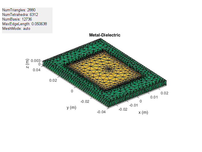
Analyze Thick Patch Antenna Performance
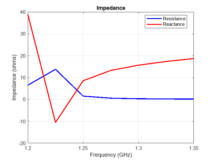
This is perhaps the most complicated case from the numerical point of view - a thick high-epsilon dielectric with significant fringing fields close to the patch edges[1]. The figure below shows the impedance plot of the antenna with resonance close to 1.22 GHz. The paper shows a resonance close to 1.27 GHz.
figure
impedance(pb2,linspace(1.2e9,1.35e9,7))
Below is the mesh used for calculating the antenna performance.
figure
mesh(pb2)
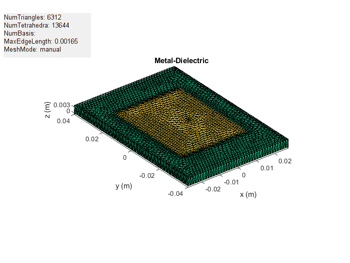
To improve the result refine the mesh. The mesh can be refined using the maximum edge length criteria. In the case below the maximum edge length is set to 1.65 mm. As can be seen below, over 12000 Tetrahedra are generated. As the mesh is very fine, the results take a longer time to compute and hence are saved in a MAT file.
figure
mesh(pb2,MaxEdgeLength=0.00165)
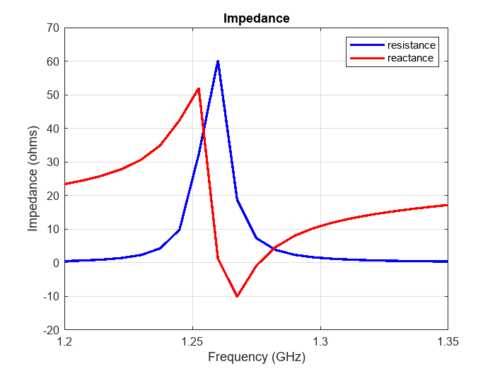
Plotting the impedance shows the resonance close to 1.27 GHz as expected.
load thickpatch
figure
plot(freq*1e-9,real(Z),'b',freq*1e-9,imag(Z),'r',LineWidth=2);
legend("resistance","reactance");
title("Impedance");
ylabel("Impedance (ohms)");
xlabel("Frequency (GHz)");
grid on;
The directivity information for this patch is also pre-computed and stored. This can be plotted using the patternCustom function as shown below. A significant back lobe is observed for the thick patch antenna.
figure
patternCustom(D.',90-el,az);
h = title("Directivity (dBi)");
h.Position = [-0.4179, -0.4179, 1.05];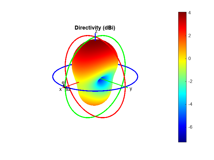
Reference
[1] Makarov, S.N., S.D. Kulkarni, A.G. Marut, and L.C. Kempel. “Method of Moments Solution for a Printed Patch/Slot Antenna on a Thin Finite Dielectric Substrate Using the Volume Integral Equation.” IEEE Transactions on Antennas and Propagation 54, no. 4 (April 2006): 1174–84. https://doi.org/10.1109/TAP.2005.872568.