High Performance DC Blocker for FPGA
This example shows how to create a DC blocking filter for a communications system by using the Biquad Filter block in DSP HDL Toolbox™.
Many communications systems use a DC blocking filter to simplify other filtering requirements. A DC blocking filter is a overall high-pass filter with a very low transition frequency that typically achieves the highpass response by subtracting a lowpass version of the input from the input, leaving just the portions of the signal above DC.
The DC blocker application is a natural fit for infinite impulse-response (IIR) filters since they are able to provide a steep transition bandwidth with fewer resources than a more common finite impulse response (FIR) filter. A drawback of an IIR filter is that stability of the filter is not guaranteed, so designs generally use a second-order section (SOS), also known as a biquad filter. Biquad filters can guarantee stability even after fixed-point quantization.
This example shows three implementations of a DC blocker algorithm for hardware. The Biquad Filter block in DSP HDL Toolbox provides options to select different SOS filter architectures to achieve different tradeoffs of resources and throughput in your design.
Reference DC Blocker Block
The Communications Toolbox™ DC Blocker Simulink block provides a behavioral reference for your hardware design. It supports four types of filters: IIR, FIR, cascaded integrator comb, and subtract mean. This example focuses on IIR filters. The block is designed for floating-point operation and has two parameters for an IIR DC blocking filter: the normalized bandwidth of the lowpass stopband and the order of the filter. The block automatically designs an SOS or biquad filter from these parameters with a passband ripple of 0.1 dB and a stopband attenuation of 60 dB.
The block uses an elliptical filter design method, which provides steeper roll-off transition bandwidth characteristics than Butterworth or Chebyshev filter designs and often allows the lowest order for a given frequency response. The downside to this type of filter is that the poles and zeros are often very close to the unit circle and the stability of a quantized filter can sometimes be challenging.
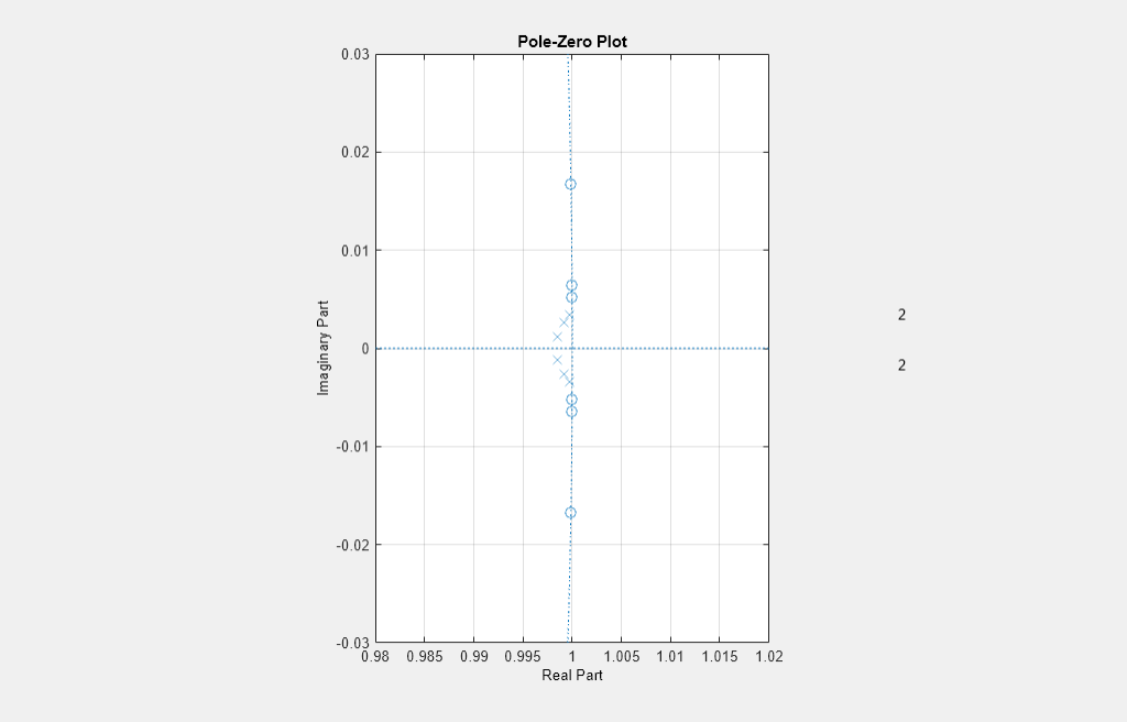
When you design SOS or biquad filters, use a design method that returns zeros, poles, and gain, (z,p,k), rather than the multiplied-out transfer function, (b,a), since the transfer function polynomial can have numerical instability. The DC Blocker block returns zeros, poles, and gain similar to this filter design code. The poles in the pole-zero plot (represented by x values) are very near but still inside the unit circle, making the double-precision filter stable.
filterOrder = 6;                        % user set, default value
normalizedBandwidth = 0.001;            % user set, default value
passbandRipple = 0.1;                   % non-settable, in dB
stopbandAtten  = 60;                    % non-settable, in dB
[z,p,k] = ellip(filterOrder,passbandRipple,stopbandAtten,normalizedBandwidth);
[numerator,denominator,scaleValues] = zp2ctf(z,p,k);
f1 = filterAnalyzer(numerator,denominator);
f2 = filterAnalyzer(numerator,denominator,Analysis="polezero");

To zoom in on the poles, use this command:
zoom(f2,"xy",[0.98 1.02 -0.03 0.03]);
Design Filter for Hardware
Quantizing the numerator and denominator coefficient independently allows for better results, so this code separates the numerator and denominator before quantization. This design has 12-bit input and targets a typical DSP element in an FPGA, so the example uses 20-bits for numerator and denominator coefficients. The pole-zero plot shows the quantized fixed-point numerator and denominator coefficients after they are converted back to double data type for analysis. You can confirm that the quantized filter is stable by changing the Analysis setting in the Filter Visualization Tool to Filter Info.
f3 = filterAnalyzer(double(fi(numerator,1,20)),double(fi(denominator,1,20)),Analysis="polezero");

To zoom in on the poles, use this command:
zoom(f3,"xy",[0.98 1.02 -0.03 0.03]);
The example model shows three different modes of the Biquad Filter block as well as the behavioral model of the DC Blocker from the Communications Toolbox library.
modelname = 'DCBlockerHDL';
open_system(modelname);
set_param(modelname,'SampleTimeColors','on');
set_param(modelname,'SimulationCommand','Update');
set_param(modelname,'Open','on');
set(allchild(0),'Visible','off');
The DF2T subsystem contains a Biquad Filter block with the Filter structure parameter set to Direct form II transposed.
The Pipe subsystem contains a Biquad Filter block with the Filter structure parameter set to Pipelined feedback form.
The FramePipe subsystem also contains a Biquad Filter block with the Filter structure parameter set to Pipelined feedback form. This subsystem uses 4-sample vector input to parallelize the filter operation and increase throughput.
In each of the subsystems, the result of the Biquad Filter is subtracted from the input data delayed to match the latency of the filter. All of the subsystems compute the same results, but each filter uses different hardware resources and synthesizes to a different clock rate. The rest of this example compares the resources, clock rate, and throughput of each of the biquad filter structures.
Direct Form II Transposed Filter Structure
To create a unique folder for the generated HDL code for each filter implementation, add the TargetDirectory name-value argument to the makehdl function call. Use this command to generate HDL code for the direct-form transposed filter.
makehdl('DCBlockerHDL/DF2T','TargetDirectory','df2t');
This figure shows the AMD® Vivado® synthesis results for the DF2T filter implementation. The synthesis targeted 200 MHz operation by specifying a 5 ns clock period, but the post-synthesis timing report shows that the minimum achievable clock period is only 6.754 ns or around 148 MHz. The critical path in this filter implementation goes through a DSP block, which is efficient use of hardware resources, but does not meet the 5 ns target.

The resource utilization for this filter structure, which has three second-order sections and one gain value, is 24 DSP elements, with 6 in the denominator and 18 in the numerator. The synthesis tool implemented the gain using shift-and-add logic.

Pipelined Feedback Filter Structure for Higher Clock Rate
The pipelined structure creates a new denominator that has higher powers in Z (that is, more delay). This new denominator introduces more poles in the filter but these poles are canceled by a modified numerator. The new poles are created from the roots of the original denominator raised to a power determined by the amount of pipelining required. Since the poles are less than one for a stable filter, the new poles are smaller than the starting values, which adds to filter stability. This structure usually results in higher synthesis clock rates because of the additional pipelining. Use this command to generate HDL code for the pipelined feedback filter.
makehdl('DCBlockerHDL/Pipe','TargetDir','pipe');
The post-synthesis timing report shows that the design has a minimum clock period of 3.142 ns or around 318 MHz, which is more than twice the speed of the DF2T version. Since this filter processes one sample per clock, this rate corresponds to 318 megasamples/s.

The resource utilization for this filter structure uses 84 DSP elements. There are 6 DSPs in the denominator and 18 DSPs in the numerator as before, and the new numerators (one per section) that cancel the added poles in the denominator use 60 DSP elements in total.

Pipelined Filter with Frame Input for Highest Clock Rate
This filter implementation increases throughput by using the frame input and output mode. This mode goes by many names including frame-based, vector, and super-sample-rate (SSR). All of these names mean that the algorithm processes more than one sample per clock cycle. You can use the buffer block in Simulink to switch between input sizes and try different designs. The model in this example is configured for four samples per clock. Use this command to generate HDL code for the pipelined feedback filter with frame-based input.
makehdl('DCBlockerHDL/FramePipe','TargetDir','framepipe');
The post-synthesis timing report shows that the achievable clock rate for the four-sample-per-clock implementation is around 275 MHz.

The critical path for this implementation is in the pipelined addition of the modified numerator, which has large word lengths due to the fixed-point requirements of this particular filter design.

Even with the lower clock rate, the throughput per clock is four times larger so this design processes about 1.1 gigasample/s.
The resource utilization for this filter structure shows that this filter uses 510 DSP elements and many more CLB elements as well. This increase is because the size of the new numerator added to cancel poles in the expanded denominator scales with the number of samples per cycle.

The pipeline depth for the Biquad Filter block in this mode is 4 pipeline stages per multiply and one pipeline stage for every addition. For a given number of samples per clock, FrameSize, the size of the new numerator is 2*FrameSize*4-1. For a frame size of 4, the new numerator has 31 taps.
Going Further
If you explore filter stability by quantizing the numerator and denominator using 16 bits instead of 20 bits, you can see that the filter becomes unstable. The filter coefficients in this example actually require a minimum word length of 19 bits for a stable filter.
You can try different frame sizes to increase throughput. As the frame size increases, the denominator coefficients get smaller and the filter numerics become more challenging. If the coefficients are quantized to zero, the Biquad Filter block issues a warning. Sometimes, increasing the word length for the denominator is the only way to avoid numeric problems since the scale of the two internally computed coefficients can differ by more than the word length you select.
At some point, the size of the logic added to handle a larger frame size exceeds the size of an equivalent FIR filter. In this design, you can experiment with the transition bandwidth for an FIR filter, starting from the normalized frequency used to design the IIR filter of 0.001. An FIR filter that matches that frequency specification has over 5000 taps and consumes considerably more resources than the IIR filter in the Biquad Filter block.