Transmit and Receive Tones Using AD9361 Dual-Channels
This example shows how to design, simulate, and deploy a dual-channel application system with the AD9361 RF card using SoC Blockset™ targeted on the Xilinx® Zynq® UltraScale+™ MPSoC ZCU102 Evaluation Kit. In this example, you generate tones using NCO, transmit them through the AD9361 channels, loop them back, and verify the received signals. You can use this example as a reference for designing systems with AD9361 dual channels for applications such as MIMO.
Supported Hardware Platforms
Xilinx Zynq UltraScale+ MPSoC ZCU102 Evaluation Kit and FMCOMMS2/3 evaluation board
Xilinx Zynq 7000 SoC ZC706 Evaluation Kit and FMCOMMS2/3 evaluation board
ZedBoard™ and FMCOMMS2/3 evaluation board
Supported Tools
SoC Blockset Support Package for AMD® FPGA and SoC Devices
Design Task and System Specification
Consider a wireless application that transmits and receives two signals using the dual channels of the AD9361 RF card. In this example, the design task involves generating two sinusoidal tones from the FPGA and configuring the FMCOMMS2/3/4 transmitter and receiver blocks to support a dual-channel transceiver. Loop back the transceivers, and receive the data back into the FPGA on the ZCU102 evaluation kit with an RF carrier frequency of 500 MHz.
Design Using SoC Blockset
Create an soc_AD9361DualChannel_top SoC model as the top model and set Hardware Board to Xilinx Zynq UltraScale+ MPSoC ZCU102 Evaluation Kit. This model includes the soc_AD9361DualChannel_fpga FPGA model and the soc_AD9361DualChannel_proc processor model, both instantiated as model references. The top model also includes the AXI4-Stream to Software block, which shares the external memory between the FPGA and the processor.
open_system('soc_AD9361DualChannel_top')
![]()
close_system('soc_AD9361DualChannel_top')
AD9361 Tx and AD9361 Rx Configuration
The AD9361 Tx and AD9361 Rx blocks are connected to the programmable logic. These blocks provide an interface to the FPGA algorithm in Simulink® for modeling a wireless system destined for implementation on a Zynq device with an FMCOMMS2/3 RF card.
For dual-channel support, enable both channels and configure the blocks as shown below.

Hardware Logic Design
The soc_AD9361DualChannel_fpga FPGA model contains two subsystems: Tx Channel, which is connected to the DAC portion of the AD9361 Tx block, and Trigger Capture, which is connected to the ADC portion.
open_system('soc_AD9361DualChannel_fpga')
![]()
close_system('soc_AD9361DualChannel_fpga')
The Tx Channel subsystem generates two complex sinusoidal waveforms using two NCO blocks. Each NCO block is configured with a different frequency using separate Phase Increment registers from the processor.
The Trigger Capture subsystem uses trigger and capture logic to capture ADC RF samples and sends the data to the processor to display the captured signal. The TriggerFrequency register from the processor controls this trigger and capture logic.
Processor Logic Design
The processor logic contains an event-based task driven by the arrival of data from the FPGA through DDR memory. The processor algorithm task, denoted as dataTask in the Task Manager block, is specified to be event-driven. The Task Manager block schedules data asynchronously using the buffer-ready event rdEvent in the memory, which signals the arrival of a frame of data from the FPGA. The algorithm itself is modeled within the Processor Algorithm Wrapper subsystem in the soc_AD9361DualChannelproc processor model and is connected to the Task Manager block at the top level. To operate on the data received as a frame of four packed samples with the uint64 data type, you must first unpack the samples and restore the signedness of the two-channel data. Each packed frame includes two samples for each channel. The output of the Processor Algorithm Wrapper subsystem is then connected to the Spectrum and Time scopes for both channels to enable visualization. In a separate Initialize Function subsystem, various registers in the FPGA subsystems are initialized with their default values. Additionally, within the same Initialize Function subsystem, the RF configuration blocks (Zynq FMCOMMS2/3/4 Transmitter and Zynq FMCOMMS2/3/4 Receiver) are configured to meet the system requirements. These blocks are configured as shown below.

open_system('soc_AD9361DualChannel_proc')
![]()
close_system('soc_AD9361DualChannel_proc')
Simulate
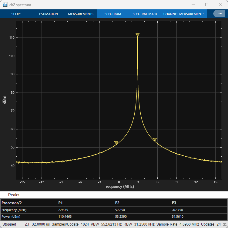
Run the model. The sinusoidal tones generated by the FPGA are sent to the AD9361 RF Card. The waveform is looped back from the FPGA to the processor through the RF card, and the ADC Capture subsystem in the FPGA captures the waveform. In the processor system, the waveform is visualized in the frequency domain using Spectrum Analyzer blocks named ch1 spectrum and ch2 spectrum. The data is observed on the spectrum scope with a substantial delay after the simulation starts. This delay is due to the time it takes for the first frame of data to become available through DDR4 to the scope, which is a result of the length of the loopback data path. The transmitted and received signals have tones of 2 MHz for channel 1 and 3 MHz for channel 2.

Implement and Run on Hardware
Hardware Setup
Connect the FMCOMMS2/3 card to the ZCU102 evaluation kit at the FMC interface. Connect the SMA connectors on the RF card to complete the loopback between Tx Channel 1, Rx Channel 1 and Tx Channel 2, Rx Channel 2.
To implement the model on a supported SoC board, use the SoC Builder tool. Ensure that the Hardware Board is set to Xilinx Zynq UltraScale+ MPSoC ZCU102 Evaluation Kit in the System on Chip tab of the Simulink toolstrip.
To open SoC Builder, click Configure, Build, & Deploy. After the SoC Builder tool opens, follow these steps.
On the Setup screen, select Build model. Click Next.
On the Select Build Action screen, select Build and load for external mode. Click Next.
On the Select Project Folder screen, specify the project folder. Click Next.
On the Review Hardware Mapping screen, click Next.
On the Review Memory Map screen, to view the memory map, click View/Edit. Click Next.
On the Validate Model screen, to check the compatibility of the model for implementation, click Validate. Click Next.
On the Build Model screen, to begin building the model, click Build. An external shell opens when FPGA synthesis begins. Click Next.
On the Connect Hardware screen, to test the connectivity of the host computer with the SoC board, click Test Connection. To go to the Run Application screen, click Next.
The FPGA synthesis can take more than 30 minutes to complete. To save time, you can use the provided pregenerated bitstream by following these steps.
Close the external shell to terminate the FPGA synthesis.
Copy the pregenerated bitstream to your project folder by entering this command at the MATLAB command prompt.
copyfile(fullfile(matlabshared.supportpkg.getSupportPackageRoot,
'toolbox','soc','supportpackages','xilinxsoc','xilinxsocexamples',
'bitstreams','soc_AD9361DualChannel_top-zcu102.bit'),'./soc_prj');
Click Load and Run to load the pregenerated bitstream and run the model on the SoC board.
After the bit file is loaded, open the generated software model.

Run the model in external mode by clicking Monitor & Tune. You can control the configuration from the Simulink model. Copy the spectrum analyzers from the top model, connect them to the rate transition blocks as this figure shows, and run the model. The spectrum analyzers display the received signal waveforms with a frequency of 2 MHz for channel 1 and 3 MHz for channel 2.
Implementation on ZC706 or ZedBoard
To implement the model on a supported board other than ZCU102 evaluation kit, first configure the model to the supported board. In the Simulink toolstrip, on the System on Chip tab, set Hardware Board to match your board.
Next, click Configure, Build, & Deploy on the toolstrip to open SoC Builder and follow the steps as previously stated for ZCU102 evaluation kit above. Generate the bitstream for your board. Load this generated bitstream and run the model on the SoC board.
Summary
In this example, you design the dual-channel data path between the FPGA, the AD9361 RF card, and design the AD9361 dual-channel RF configuration from the processor using FMCOMMS2/3/4 blocks on the Xilinx Zynq UltraScale+ MPSoC ZCU102 Evaluation Kit. You design a system that generates two sinusoidal waveforms, which are sent to the AD9361 dual channels and looped back at AD9361 RF level. The system captures the received sine wave samples and sends them to MATLAB host through the processor to display the captured sine wave signals. You can use this dual-channel design example as a reference for designing a two-channel MIMO system.
See Also
AD9361 Rx | AD9361 Tx | Zynq and FMCOMMS2/3/4 Receiver Configuration | Zynq and FMCOMMS2/3/4 Transmitter Configuration